55 Products found
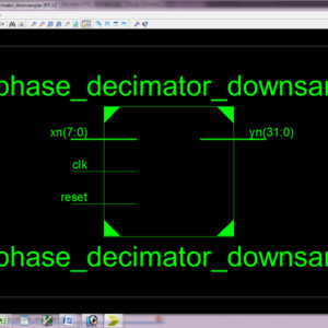
To develop and Implement Low Power, High Speed VLSI for Processing Signals using Multi rate Techniques Low Power Divider Using Vedic Mathematics
Abstract:
Multirate technique is necessary for systems with different input and output sampling rates. Recent advances in mobile computing and communication applications demand low power and high speed VLSI DSP systems. In this paper to discuss the downsampling technique and its improvement, major drawbacks of present approaches possible to increase degeneracy. This Multirate design methodology is systematic and applicable to many problems. The proposed architecture of this paper analysis the logic size, area and power consumption using Xilinx 14.2.The proposed architecture of this paper analysis the logic size, area and power consumption using Xilinx 14.2.
List of the following materials will be included with the Downloaded Backup:
High Speed Area Efficient VLSI Architecture of Three Operand Binary Adder
Abstract:
Three-operand binary adder is the basic functional unit to perform the modular arithmetic in various cryptography and pseudorandom bit generator (PRBG) algorithms. Carry save adder (CS3A) is the widely used technique to perform the three-operand addition. However, the ripple-carry stage in the CS3A leads to a high propagation delay of O(n). Moreover, a parallel prefix two-operand adder such as Han-Carlson (HCA) can also be used for three-operand addition that significantly reduces the critical path delay at the cost of additional hardware. Hence, a new high-speed and area-efficient adder architecture is proposed using pre-compute bitwise addition followed by carry prefix computation logic to perform the three-operand binary addition that consumes substantially less area, low power and drastically reduces the adder delay to O(log2 n). The proposed architecture is implemented on the FPGA device for functional validation and also synthesized with the commercially available 32nm CMOS technology library. The post-synthesis results of the proposed adder reported 3.12, 5.31 and 9.28 times faster than the CS3A for 32-, 64- and 128- bit architecture respectively. Moreover, it has a lesser area, lower power dissipation and smaller delay than the HC3A adder. Also, the proposed adder achieves the lowest ADP and PDP than the existing three-operand adder techniques.
List of the following materials will be included with the Downloaded Backup:
Design and analysis of High speed Wallace tree multiplier using parallel prefix adders for VLSI circuit designs
Abstract:
Major operation block in any processing unit is a multiplier. There are many multiplication algorithms are proposed, by using which multiplier structure can be designed. Among various multiplication algorithms, Wallace tree multiplication algorithm is beneficial in terms of speed of operation. With the advancement of technology, demand for circuits with high speed and low area is increasing. In order to improve the speed of Wallace tree multiplier without degrading its area parameter, a new structure of Wallace tree multiplier is proposed in this paper. In the proposed structure, the final addition stage of partial products is performed by parallel prefix adders (PPAs). In this paper, five Wallace tree multiplier structures are proposed using Kogge stone adder, Sklansky adder, Brent Kung adder, Ladner Fischer adder and Han carlson adder. All the multiplier structures are designed using Verilog HDL in Xilinix 13.2 design suite. The proposed structures are simulated using ISIM simulator and synthesized using XST synthesizer. The proposed designs are analyzed with respect to traditional multiplier design in terms of area (No. of LUTs) and delay (ns).
List of the following materials will be included with the Downloaded Backup: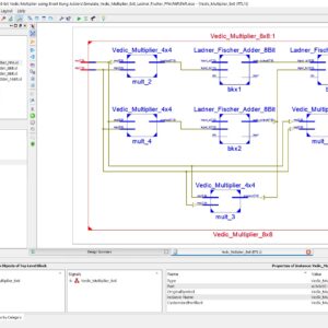
Design of High Speed 8-bit Vedic Multiplier using Brent Kung Parallel Prefix Adder
Base Paper Abstract:
One of the primary purposes of a digital signal processing system is multiplication. The multiplier’s performance affects the DSP system’s overall performance. Therefore, it is crucial to create an effective and quick multiplier implementation design. Vedic mathematics can be used to simplify complex computations so that they are easier to perform verbally. Urdhva Triyambakam is the multiplication algorithm used in Vedic math. In this paper, we employing Brent Kung adder to enhance the Vedic multiplier’s performance. The Urdhva Tiryagbhyam sutra is being used in place of other multiplication strategies since it applies to all instances of algorithms for N x N bit numbers and produces the least amount of latency. Four 4-bit vedic multipliers, two 8-bit Brent Kung adders, one 4-bit Brent Kung adder, and an OR gate are used to create an 8-bit vedic multiplier. A 4-bit vedic multiplier is created similarly by combining four 2-bit vedic multipliers, two 4-bit Brent Kung Adders, one 2-bit Brent Kung Adder, and one OR gate. These four-bit vedic multipliers are then combined to form an eight-bit vedic multiplier. After that, Xilinx Vivado Software is used to simulate and synthesis the 8 x 8 Vedic Multiplier, which was coded in Verilog HDL. The proposed Vedic Multiplier is outperformed in terms of speed when compared to related works.
List of the following materials will be included with the Downloaded Backup: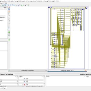
FPGA Implementation of Single Precision Floating Point Multiplier using High Speed Parallel Prefix Adder based Wallace Tree Multiplier
Base Paper Abstract:
In this paper present, an efficient implementation of single precision method of floating point multiplier target for Xilinx Vertex 5 FPGA using Verilog HDL. The floating point implementation will cover up with 23-bit exponent, 8-bit mantissa, and 1 sign bit. This proposed architecture implement with high speed parallel prefix adder based Wallace Tree Multiplier. a Wallace tree multiplication will provide effective terms of low logic sizes and more speed of operations. In a recent arithmetic applications based circuit design will have more demand with high speed and low area, in this manner the proposed approach of this work will improve the speed of Wallace tree multiplier using 4:2 compressor method without degrading its area parameter. Thus, the proposed method will integrate more efficient and more reliable Kogge stone parallel prefix, Brent kung parallel prefix, Sklansky parallel prefix addition operation in the Wallace tree multiplication on final addition stage at 16-bit data width. Finally, done this floating point multiplier architecture with Wallace tree architecture included normalized rounding method and to reduce area, delay and power. The error difference will have analyzed using Modelsim Software, and analyses optimized logic size's, delay and power consumptions.
List of the following materials will be included with the Downloaded Backup:
A High-Speed FPGA-based True Random Number Generator using Metastability with Clock Managers
Base Paper Abstract:
True random number generators (TRNGs) are fundamentals in many important security applications. Though they exploit randomness sources that are typical of the analog domain, digital-based solutions are strongly required especially when they have to be implemented on Field Programmable Gate Array (FPGA)-based digital systems. This paper describes a novel methodology to easily design a TRNG on FPGA devices. It exploits the runtime capability of the Digital Clock Manager (DCM) hardware primitives to tune the phase shift between two clock signals. The presented auto-tuning strategy automatically sets the phase difference of two clock signals in order to force on one or more flip-flops (FFs) to enter the metastability region, used as a randomness source. Moreover, a novel use of the fast carry-chain hardware primitive is proposed to further increase the randomness of the generated bits. Finally, an effective on-chip post-processing scheme that does not reduce the TRNG throughput is described. The proposed TRNG architecture has been implemented on the Xilinx Zynq XC7Z020 System on Chip (SoC). It passed all the National Institute of Standards and Technology (NIST) SP 800-22 statistical tests with a maximum throughput of 300×106 bit per second. The latter is considerably higher than the throughput of other previously published DCMbased TRNGs.
List of the following materials will be included with the Downloaded Backup:
An Efficient and High Speed Overlap Free Karatsuba Based Finite Field Multiplier for FPGA Implementation
Abstract:
Cryptography systems have become inseparable parts of almost every communication device. Among cryptography algorithms, public-key cryptography, and in particular elliptic curve cryptography (ECC), has become the most dominant protocol at this time. In ECC systems, polynomial multiplication is considered to be the most slow and area consuming operation. This article proposes a novel hardware architecture for efficient field-programmable gate array (FPGA) implementation of Finite field multipliers for ECC. Proposed hardware was implemented on different FPGA devices for various operand sizes, and performance parameters were determined. Comparing to state-of-the art works, the proposed method resulted in a lower combinational delay and area–delay product indicating the efficiency of design.
List of the following materials will be included with the Downloaded Backup:
FPGA Based High Definition SPWM Generation With Harmonic Mitigation Property
Abstract:
High-resolution sinusoidal pulse width modulation (SPWM) switching is beneficial in order to achieve compact size and fine sinusoidal output of dc–ac converters. In this article, a novel field-programmable gate array (FPGA) based high-definition SPWM (HD-SPWM) architecture is proposed for adopting a scheme of integrating a lower frequency PWM train to a high-frequency SPWM train in order to suppress inverter output harmonics while achieving high resolution output. An optimized FPGA based two-stage finite-state-machine (FSM) architecture is designed, where the initial stage decides pulse widths of a lower frequency PWM train based on the premeditated pulse width of the high-frequency SPWM train, whereas in the final stage, lower frequency PWM pulse widths are integrated with the high-frequency SPWM pulse widths to generate updated pulse widths of high-frequency SPWM, i.e., HD-SPWM. Moreover, a pre-formulation mathematical model is established for the calculation of duty-cycle count values of pulse trains to support the online adjustment of modulation index (MI) of the HD-SPWM. The proposed generation has the benefits of harmonic mitigation, online fine adjustment of MI, low-processing time, and requirement of a minor segment of a medium-sized FPGA; thereby, providing a good tradeoff between larger designs and higher performance. Theoretical calculations, characteristics, and design contemplations are specified, and the HD-SPWM generation is demonstrated through experimentation with a Xilinx Spartan-3 FPGA board.
List of the following materials will be included with the Downloaded Backup:
A Low Power and High Speed Voltage Level Shifter Based on a Regulated Cross Coupled Pull Up Network
Abstract:
In this brief, a fast and very low power voltage level shifter (LS) is presented. By using a new regulated cross-coupled (RCC) pull-up network, the switching speed is boosted and the dynamic power consumption is highly reduced. The proposed (LS) has the ability to convert input signals with voltage levels much lower than the threshold voltage of a MOS device to higher nominal supply voltage levels. The presented LS occupies a small silicon area owing to its very low number of elements and is ultra-low-power, making it suitable for low-power applications such as implantable medical devices and wireless sensor networks. Results of the post-layout simulation in a standard 0.18-μm CMOS technology show that the proposed circuit can convert up input voltage levels as low as 80 mV. The power dissipation and propagation delay of the proposed level shifter for a low/high supply voltages of 0.4/1.8 V and input frequency of 1 MHz are 123.1 nW and 23.7 ns, respectively.
List of the following materials will be included with the Downloaded Backup:
A High-Performance Multiply-Accumulate Unit by Integrating Additions and Accumulations into Partial Product Reduction Process
Abstract:
In this paper, we propose a low-power high-speed pipeline multiply-accumulate (MAC) architecture. In a conventional MAC, carry propagations of additions (including additions in multiplications and additions in accumulations) often lead to large power consumption and large path delay. To resolve this problem, we integrate a part of additions into the pa rtial product reduction (PPR) process. In the proposed MAC architecture, the addition and accumulation of higher significance bits are not performed until the PPR process of the next multiplication. To correctly deal with the overflow in the PPR process, a small-size adder is designed to accumulate the total number of carries. Compared with previous works, experimental results show that the proposed MAC architecture can greatly reduce both power consumption and circuit area under the same timing constraint.
List of the following materials will be included with the Downloaded Backup:
FPGA implementation of low power and high speed image edge detection algorithm
Abstract:
Image processing is a vital task in data processing system for applications in medical fields, remote sensing, microscopic imaging etc., Algorithms for processing image exist except for real time system style, hardware implementation is most popular principally. This paper presents a design for Sobel filter based edge detection on Field Programmable Gate Array (FPGA) board. Hardware implementation of the Sobel edge detection algorithm is chosen because it presents an honest scope for similarity over software package. On the opposite hand, Sobel edge detection will work with less deterioration in high level of noise. Edges are primarily the noticeable variation of intensities in a picture. Edges facilitate to spot the placement of an object and also the boundary of a selected entity within the image. It conjointly helps in feature extraction and pattern recognition. Hence, edge detection is of nice importance in pc vision. The planned design for edge detection exploitation Sobel algorithm is designed using structural Verilog lipoprotein synthesized exploitation Cadence Genus and enforced using Cadence Innovus. The practicality of the planning is verified exploitation normal pictures by FPGA implementation. The proposed architecture reduce the power, delay and space complexity compare to three existing architectures.
List of the following materials will be included with the Downloaded Backup:
High-Speed Hybrid-Logic Full Adder Using High-Performance 10-T XOR–XNOR Cell
Abstract:
Hybrid logic style is widely used to implement full adder (FA) circuits. Performance of hybrid FA in terms of delay, power, and driving capability is largely dependent on the performance of XOR–XNOR circuit. In this article, a high speed, low-power 10-T XOR–XNOR circuit is proposed, which provides full swing outputs simultaneously with improved delay performance. The performance of the proposed circuit is measured by simulating it in cadence virtuoso environment using 90-nm CMOS technology. The proposed circuit reduces the power delay product (PDP) at least by 7.5% than that of the available XOR–XNOR modules. Four different designs of FAs are also proposed in this article utilizing the proposed XOR–XNOR circuit and available sum and carry modules. The proposed FAs provide 2%–28.13% improvement in terms of PDP than that of other architectures. To measure the driving capabilities, the proposed FAs are embedded in 2-, 4-, and 8-bit cascaded full adder (CFA) structures. Results show that two of the proposed FAs provide the best performance for a higher number of bits among all the FAs.
List of the following materials will be included with the Downloaded Backup:
A Highly Efficient Conditional Feed through Pulsed Flip Flop for High Speed Applications
Abstract:
A novel type of highly efficient conditional feed through pulse-triggered flip-flop (P-FF) is proposed and demonstrated. The data-to-output (D-to-Q) delay in this circuit was highly optimized using pre discharging and conditional signal feed through schemes. Power consumption was also reduced using a shared pulse generator and an output feedback-controlled conditional keeper, which diminished the floating status of the internal node. The driving strength of this design was further enhanced by including an additional pull-down path at the output node. Various post layout simulation results applied to 16-nm Fin FET technology demonstrated a higher energy efficiency (at all input data toggle rates) for the proposed topology than comparable P-FF devices. Notably, the proposed model achieved a 62% D-to-Q delay reduction, compared to a transmission gate FF, outperforming the device by more than 66% in terms of power efficiency and 87% in energy efficiency (at a 50% input data toggle rate). Improvements were even more significant in comparison with other conventional P-FFs. These results suggest the proposed design to be a viable new option for high-efficiency sequential elements in high-speed applications.
List of the following materials will be included with the Downloaded Backup:
Low Power and High Speed Implementation of FIR filter design using CMOS GDI Truncated Multiplier
Abstract:
The logic size, propagation delay, power of applications, based upon this improvement the adder design logic size will reduced year by year, here a proposed In recent technology of any application, adders is a more priority to do a function and task of arithmetic operation, in crucial this adder based arithmetic operation will decide work of this paper will design using a single bit full adder to design a multiplier. In this multiplier design, adder is a main priority to reduce the arithmetic logic size and increases speed of multiplier, in recent we have lots of multiplier design, Vedic multiplier, Wallace tree multiplier, booth multiplier, approximate multiplier. Here, the proposed work will taken truncated multiplier design, it's because, the truncated multiplier will have a capability to reduced internal and external architecture size in every design, regarding this truncated multiplier will have three options such as rounding, deleting, truncating, here the MSB bits will be truncated and present the output of n x n multiplication will provided only n bit level, using this truncated multiplier the proposed work will designed a 8-Tap FIR(Finite impulse response) filter and shown the efficiency of filter design using this CMOS GDI (Gate Diffusion Input) adder design. This proposed work will design in CMOS Logic gate and which 10-T transistor level of full adders with 90um technology, finally proved the terms of area, delay and power.
List of the following materials will be included with the Downloaded Backup:
High speed and low power preset-able modified TSPC D flip-flop design and performance comparison with TSPC D flip-flop
Abstract:
Positron emission tomography (PET) is a nuclear functional imaging technique that produces a three-dimensional image of functional organs in the body. PET requires high resolution, fast and low power multichannel analog to digital converter (ADC). A typical multichannel ADC for PET scanner architecture consists of several blocks. Most of the blocks can be designed by using fast, low power D flip-flops. A preset-able true single phase clocked (TSPC) D flip-flop shows numerous glitches (noise) at the output due to unnecessary toggling at the intermediate nodes. Preset-able modified TSPC (MTSPC) D flip flop have been proposed as an alternative solution to alleviate this problem. However, the MTSPC D flip-flop requires one extra PMOS to suspend toggling of the intermediate nodes. In this work, we designed a 7-bit preset-able gray code counter by using the proposed D flip-flop. This work involves UMC 180 nm CMOS technology for preset-able 7-bit gray code counter where we achieved 1 GHz maximum operation frequency with most significant bit (MSB) delay 0.96 ns, power consumption 244.2 μW (micro watt) and power delay product (PDP) 0.23 pJ (Pico joule) from 1.8 V power supply.
List of the following materials will be included with the Downloaded Backup:
High Performance VLSI architecture for M-PSK modems
Abstract:
M-PSK (phase shift keying) modulation schemes are used in many high-speed applications like satellite communication, as they are more bandwidth and power efficient compared with other schemes. This study presents very large scale integrated circuits (VLSI) architectures for modulators and demodulators of quadrature phase shift keying (QPSK), 4PSK, 8PSK and 16PSK systems, based on the principle of direct digital synthesis. The proposed modulators do not use any multiplier in contrast to the conventional modulators and hence they are relatively fast and area efficient. Based on the coherent detection technique, this study proposes new demodulation algorithms for 4PSK, 8PSK and 16PSK systems which can be implemented both in analogue and digital domains. This study also presents VLSI architectures for all the proposed algorithms. The proposed architectures are described in VHDL and implemented on Xilinx field programmable gate arrays (FPGAs). The simulation results verify their functional validity and implementation results show the suitability of the proposed architectures for satellite communications.
List of the following materials will be included with the Downloaded Backup:
RoBA Multiplier A Rounding Based Approximate Multiplier for High Speed yet Energy Efficient Digital Signal Processing
Abstract:
In this paper, we propose an approximate multiplier that is high speed yet energy efficient. The approach is to round the operands to the nearest exponent of two. This way the computational intensive part of the multiplication is omitted improving speed and energy consumption at the price of a small error. The proposed approach is applicable to both signed and unsigned multiplications. We propose three hardware implementations of the approximate multiplier that includes one for the unsigned and two for the signed operations. The efficiency of the proposed multiplier is evaluated by comparing its performance with those of some approximate and accurate multipliers using different design parameters. In addition, the efficacy of the proposed approximate multiplier is studied in two image processing applications, i.e., image sharpening and smoothing.
List of the following materials will be included with the Downloaded Backup:
A High Speed FPGA Implementation of an RSD Based ECC Processor
In this paper, an exportable application-specific instruction-set elliptic curve cryptography processor based on redundant signed digit representation is proposed. The processor employs extensive pipelining techniques for Karatsuba–Ofman method to achieve high throughput multiplication. Furthermore, an efficient modular adder without comparison and a highthrough put modular divider, which results in a short datapath for maximized frequency, are implemented. The processor supports the recommended NIST curve P256 and is based on an extended NIST reduction scheme. The proposed architecture of this paper analysis the logic size, area and power consumption using Xilinx 14.2.
List of the following materials will be included with the Downloaded Backup:
High Speed Low Power and Highly Reliable Frequency Multiplier for DLL Based Clock Generator
To propose a novel frequency multiplier with high-speed, low-power, and highly reliable design for a delay-locked loop-based clock generator to generate a multiplied clock with a high frequency and wide frequency range. The proposed edge combiner achieves a high-speed and highly reliable operation using a hierarchical structure and an overlap canceller. In addition, by applying the logical effort to the pulse generator and multiplication-ratio control logic design, the proposed frequency multiplier minimizes the delay difference between positive- and negative-edge generation paths, which causes a deterministic jitter. Finally, a numerical analysis is performed to analyze and compare the performance of the proposed frequency multiplier with that of previous frequency multipliers. The proposed frequency multiplier is fabricated using a 0.13-µm CMOS process technology, and has the multiplication ratios of 1, 2, 4, 8, and 16, and an output range of 50 MHz–3.3 GHz. The frequency multiplier achieves power consumption is 17.49mW. The proposed architecture of this paper is analysis the logic size, area and power consumption using tanner tool.
List of the following materials will be included with the Downloaded Backup:
Low-Cost High-Performance VLSI Architecture for Montgomery Modular Multiplication
Source Code : VHDL & VERILOG HDL
Abstract: This paper proposes a simple and efficient Montgomery multiplication algorithm such that the low-costand high-performance Montgomery modular multiplier can be implemented accordingly. The proposed multiplier output data with representation and uses only one parallel prefix adder to avoid a carry propagation and reduce the area, power and delay, and also increasing the speed. Mainly the usage of parallel prefix adder is to reduce the significant delay reduction and area × time2 improvements, all this at the cost of higher power consumption, which is the main reason preventing the use of parallel-prefix adders to achieve high-speed reverse converters in nowadays systems. Hence, to solve the high power consumption problem, novel specific hybrid parallel-prefix-based adder components those provide better trade-off between delay and power consumption. As a result, the extra clock cycles for operand pre-computation and format conversion can be hidden and high throughput can be obtained. Experimental results show that the proposed Montgomery modular multiplier can achieve higher performance and significant area–time product improvement when compared with previous designs. Using VHDL to design the RTL, and the result to be shown in Xilinx 14.2 with Power consumption and area reduction.
List of the following materials will be included with the Downloaded Backup:
Design and Implementation of an 8-bit Approximate Wallace Tree Multiplier for Energy Efficient Deep Neural Networks
Base Paper Abstract:
Approximate arithmetic computing circuits and architectures have been proven to be energy efficient designs for Deep Neural Networks (DNNs) which are error resilient. In this paper, an approximate 8-bit Wallace Multiplier has been proposed and designed in 90nm CMOS technology for energy efficiency. The proposed 8-bit approximate multiplier design consumes ~32% less energy in comparison to an accurate 8-bit Wallace Tree multiplier with less than 20% Mean Relative Error (MRE).
List of the following materials will be included with the Downloaded Backup:
An Efficient Image Encryption Algorithm Based on Innovative DES Structure and Hyperchaotic Keys
Base Paper Abstract:
In fact, as a traditional encryption method, DES has been certified as an unsuitable tool for ciphering due to its smaller key space. Further, in concern of the real-time encryption in the current fast communication era, such as 5G, long-time as well as large computational level processes are not gotten into the consideration. As a result, an innovative encryption structure with hyperchaotic keys for efficient encryption is constructed, where the frame of DES structure is applied, the plain image is shuffled through row and column directions in the first round, and then rearranged to be 64 blocks to fit into the frame of DES structure for 4 rounds ciphering with hyperchaotic subkeys. Also, in order to encrypt the content of the image at the block level, a set of alternative S-box has been produced in this article as well. The simulation results indicate that the proposed scheme is feasible and reliable for digital image encrypting, not only a large key space can be obtained, but also the low correlation of the adjacent contents can be achieved, and further, in comparison of several existing approaches, less-computational resource can be proven as well. In particular, due to the innovative DES structure, the computational speed is significantly faster than the original DES algorithm and many other chaos-based image ciphering schemes.
List of the following materials will be included with the Downloaded Backup:
FPGA Implementation of 64 Block Data Encryption Standard Algorithm
Proposed Abstract:
The Data Encryption Standard (DES) is widely recognized as the inaugural and prevailing symmetric key method used for the cryptographic processes of encrypting and decrypting digital data. Despite its lack of security against determined attackers in contemporary times, the use of this method persists in older systems. This work introduces a novel implementation of the Data Encryption and Decryption Standard algorithm using Field Programming Gate Arrays (FPGAs) that prioritizes security, high throughput, and space efficiency. The suggested solution involves the creation of a system that utilizes a block size of 64 bits and a key length that is also 64 bits. Additionally, the system operates with a data width of 64 bits. This achievement is accomplished by integrating the notion of pipelining with time variable permutations, and then comparing it with previously shown encryption techniques. The permutations undergo temporal variations under the control of the cryptographer. Hence, the cipher text also undergoes alteration while the key and plaintext remain constant. The algorithm under consideration has been successfully executed on the Xilinx Vetex-5 Field-Programmable Gate Array (FPGA) platform. The findings of this study indicate that the suggested implementation exhibits exceptional speed in comparison to other hardware implementations. Additionally, it demonstrates superior area efficiency and significantly enhanced security measures.
List of the following materials will be included with the Downloaded Backup:
Optimizing Ternary Multiplier Design with Fast Ternary Adder
Base Paper Abstract:
Existing ternary multiplier designs are difficult to use in ternary systems. Thus, ternary Wallace tree multipliers that reduce the number of transistors by using 4-input ternary adders are proposed to improve the performance of existing ternary multipliers. A ternary carry-select adder is also proposed to reduce the carry propagation delay, used as a carry-chain adder of the Wallace tree. The proposed multipliers are designed with a custom ternary standard cell library synthesized by multi-threshold complementary metal-oxide-semiconductor (CMOS) with a 28 nm process. Power and delay are verified via HSPICE simulation. The proposed 36 × 36 ternary multiplier shows 79.3% power-delay product improvement over the previous ternary multiplier. The proposed 40 × 40 ternary multiplier shows a power-delay product comparable with that of the 64 × 64 binary multiplier synthesized using Synopsys Design Compiler.
List of the following materials will be included with the Downloaded Backup: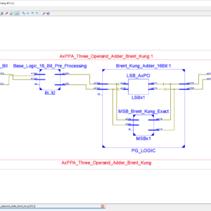
AxPPA: Approximate Parallel Prefix Adders
Base Paper Abstract:
Addition units are widely used in many computational kernels of several error-tolerant applications such as machine learning and signal, image, and video processing. Besides their use as stand-alone, additions are essential building blocks for other math operations such as subtraction, comparison, multiplication, squaring, and division. The parallel prefix adders (PPAs) is among the fastest adders. It represents a parallel prefix graph consisting of the carry operator nodes, called prefix operators (POs). The PPAs, in particular, are among the fastest adders because they optimize the parallelization of the carry generation (G) and propagation (P). In this work, we introduce approximate PPAs (AxPPAs) by exploiting approximations in the POs. To evaluate our proposal for approximate POs (AxPOs), we generate the following AxPPAs, consisting of a set of four PPAs: approximate Brent–Kung (AxPPA-BK), approximate Kogge–Stone (AxPPAKS), Ladner-Fischer (AxPPA-LF), and Sklansky (AxPPA-SK). We compare four AxPPA architectures with energy-efficient approximate adders (AxAs) [i.e., Copy, error-tolerant adder I (ETAI), lower-part OR adder (LOA), and Truncation (trunc)]. We tested them generically in stand-alone cases and embedded them in two important signal processing application kernels: a sum of squared differences (SSDs) video accelerator and a finite impulse response (FIR) filter kernel. The AxPPA-LF provides a new Pareto front in both energy-quality and area-quality results compared to state-of-the-art energy-efficient AxAs.
List of the following materials will be included with the Downloaded Backup:
Determining Application-Specific Knowledge for Improving Robustness of Sequential Circuits
Base Paper Abstract:
Due to their shrinking feature sizes as well as environmental influences, such as high-energy radiation, electrical noise, and particle strikes, integrated circuits are getting more vulnerable to transient faults. Accordingly, how to make those circuits more robust has become an essential step in today’s design flows. Methods increasing the robustness of circuits against these faults already exist for a long period of time but either introduce huge additional logic, change the timing behavior of the circuit, or are applicable for dedicated circuits such as microprocessors only. In this paper, we propose an alternative method, which overcomes these drawbacks by determining application specific knowledge of the circuit, namely the relations of flip-flops and when they assume the same value. By this, we exploit partial redundancies, which are inherent in most circuits anyway (even the optimized ones), to frequently compare the circuit signals for their correctness—eventually leading to an increased robustness. Since determining the correspondingly needed information is a computationally hard task, formal methods, such as bounded model checking, satisfiability-based automatic test pattern generation, and binary decision diagrams, are utilized for this purpose. The resulting methodology requires only a slight increase in additional hardware, does only influence the timing behavior of the circuit negligibly, and is automatically applicable to arbitrary circuits. Experimental evaluations confirm these benefits.
List of the following materials will be included with the Downloaded Backup:
Approximate Multiplier Design Using Novel Dual-Stage 4 : 2 Compressors
Base Paper Abstract:
High speed multimedia applications have paved way for a whole new area in high speed error-tolerant circuits with approximate computing. These applications deliver high performance at the cost of reduction in accuracy. Furthermore, such implementations reduce the complexity of the system architecture, delay and power consumption. This paper explores and proposes the design and analysis of two approximate compressors with reduced area, delay and power with comparable accuracy when compared with the existing architectures. The proposed designs are implemented using 45 nm CMOS technology and efficiency of the proposed designs have been extensively verified and projected on scales of area, delay, power, Power Delay Product (PDP), Error Rate (ER), Error Distance (ED), and Accurate Output Count (AOC). The proposed approximate 4 : 2 compressor shows 56.80% reduction in area, 57.20% reduction in power, and 73.30% reduction in delay compared to an accurate 4 : 2 compressor. The proposed compressors are utilised to implement 8 × 8 and 16 × 16 Dadda multipliers. These multipliers have comparable accuracy when compared with state-of-the-art approximate multipliers. The analysis is further extended to project the application of the proposed design in error resilient applications like image smoothing and multiplication.
List of the following materials will be included with the Downloaded Backup:
A Configurable Floating Point Multiple Precision Processing Element for HPC and AI Converged Computing
Abstract:
There is an emerging need to design configurable accelerators for the high-performance computing (HPC) and artificial intelligence (AI) applications in different precisions. Thus, the floating-point (FP) processing element (PE), which is the key basic unit of the accelerators, is necessary to meet multiple-precision requirements with energy-efficient operations. However, the existing structures by using high-precision-split (HPS) and low-precision-combination (LPC) methods result in low utilization rate of the multiplication array and long multi term processing period, respectively. In this article, a configurable FP multiple-precision PE design is proposed with the LPC structure. Half precision, single precision, and double precision are supported. The 100% multiplier utilization rate of the multiplication array for all precisions is achieved with improved speed in the comparison and summation process. The proposed design is realized in a 28-nm process with 1.429-GHz clock frequency. Compared with the existing multiple-precision FP methods, the proposed structure achieves 63% and 88% areasaving performance for FP16 and FP32 operations, respectively. The 4× and 20× maximum throughput rates are obtained when compared with fixed FP32 and FP64 operations. Compared with the previous multiple-precision PEs, the proposed one achieves the best energy-efficiency performance with 975.13 GFLOPS/W.
List of the following materials will be included with the Downloaded Backup:
Comparative study of 16-order FIR filter design using different multiplication techniques
Abstract:
This study represents designing and implementation of a low power and high speed 16 order FIR filter. To optimize filter area, delay and power, different multiplication techniques such as Vedic multiplier, add and shift method and Wallace tree (WT) multiplier are used for the multiplication of filter coefficient with filter input. Various adders such as ripple carry adder, Kogge Stone adder, Brent Kung adder, Ladner Fischer adder and Han Carlson adder are analyzed for optimum performance study for further use in various multiplication techniques along with barrel shifter. Secondly optimization of filter area and delay is done by using add and shift method for multiplication, although it increases power dissipation of the filter. To reduce the complexity of filter, coefficients are represented in canonical signed digit representation as it is more efficient than traditional binary representation. The finite impulse-response (FIR) filter is designed in MATLAB using equiripple method and the same filter is synthesized on Xilinx Spartan 3E XC3S500E target field-programmable gate array device using Very High Speed Integrated Circuit Hardware Description Language (VHDL) subsequently the total on-chip power is calculated in Vivado2014.4. The comparison of simulation results of all the filters show that FIR filter with WT multiplier is the best optimized filter.
List of the following materials will be included with the Downloaded Backup:
A 2.5-V 8-Bit Low power SAR ADC using POLC and SMTCMOS D-FF for IoT Applications
Abstract:
A 2.5-V 8-bit low force and efficient Successive Approximation Register Analog-to-Digital converter (SAR-ADC) utilizing a Principled Open Loop Comparator (POLC) and Switched Multi-Threshold Complementary Metal Oxide Semiconductor (SMTCMOS) D-FF shift Register. In light of high proficiency and low force applications SAR-ADC is increasingly well known, yet it experience the ill effects of resolution and speed confinements. To defeat the above issue proposed a systematic methodology uses low force POLC based SAR-ADC is structured. Considering about the resolution, speed and compact design of 8- bit SAR-ADC, the proposed POLC strategy reasonably diminishes the propagation delay by 37% and decreases the force utilization by 62% appeared differently in relation to the standard system. A D-flip flop is planned to employ SMTCMOS procedure which has low force utilization and productively decline the leakage power. All the above circuits are simulated by using TANNER-EDA tool in 0.25μm CMOS technology produces 97% Efficiency.
List of the following materials will be included with the Downloaded Backup:
Implementation of Low Power 1-bit Hybrid Full Adder using 22nm CMOS Technology
Abstract:
Adders are plays a vital role in digital and vlsi systems. Arithmetic operations are an essential part of digital systems. During VLSI systems, the entire research is on lowering the scale of transistors for enforcing any other digital system. This proposed architecture implemented by different types of logic systems; each logic performs the different role in the hybrid system. The hybrid Full Adder cell with one bit is implemented in this structure. The proposed method is investigated using 22-nm CMOS hybrid full adder. The proposed architecture demonstrates substantial efficiency in power consumption and delay, based on simulation results. The simulation result expressed that the full adder circuit is used to modern high speed central processing unit in the data path architecture. This form of hybrid Full Adder, reduces the delay and increasing efficiency and mainly used in nano technology applications. The average power consumption of 1.1055uW with moderately low delay of 7.0415 ps was found to be extremely low for 0.8-V supply at 22-nm technology. These kind of adder allocates significant improvements in power, high speed and area compared with previous full adder designs.
List of the following materials will be included with the Downloaded Backup: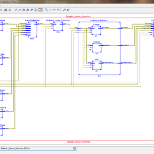
FPGA Implementation of Epileptic Seizure Detection Using ELM Classifier Detection Using ELM Classifier
Abstract:
Electroencephalography (EEG) Signals are widely used to determine the brain disorders. The Electrical activity of human brain is recorded in the form of EEG signal. The abnormal Electrical activity of the human brain is called as epileptic seizure. In epilepsy patients, the seizure occurs at unpredictable times and it causes sudden death. Detection and Prediction of Epileptic seizure is performed by analyzing the EEG signal. The EEG signal of human brain is random in nature, hence detection of seizure in EEG signal is challenging task. Hardware implementation of Epileptic seizure detection system is necessary for real time applications. In this work an accurate approach is used to identify the Epileptic seizure and that is implemented in FPGA (Field Programmable Gate Array).The hardware implementation of epileptic seizure detection algorithm is done using Xilinx System generator tool. In the first step the EEG signal is extracted from the human brain and it is filtered by using Finite Impulse response (FIR) band pass filter. The band pass filter separates the EEG signal into delta, theta, alpha, beta and gamma brain rhythms. The band separated brain signal is modeled by linear prediction theory. In the next step features are extracted from the modeled EEG signal and the classification of normal or seizure signal is done by using Extreme Learning Machine (ELM) classifier. The EEG signals used in this paper were obtained from Epilepsy Center at the University of Bonn, Germany. The hardware architecture, Look up tables, resource utilization, Accuracy and power consumption of the algorithm is analyzed using xilinx zynq7000 all programmable soc.
List of the following materials will be included with the Downloaded Backup:
Comparison and Extension of Approximate 4-2 Compressors for Low-Power Approximate Multipliers
Abstract:
Approximate multipliers attract a large interest in the scientific literature that proposes several circuits built with approximate 4-2 compressors. Due to the large number of proposed solutions, the designer who wishes to use an approximate 4-2 compressor is faced with the problem of selecting the right topology. In this paper, we present a comprehensive survey and comparison of approximate 4-2 compressors previously proposed in literature. We present also a novel approximate compressor, so that a total of twelve different approximate 4-2 compressors are analyzed. The investigated circuits are employed to design 8 × 8 and 16 × 16 multipliers, implemented in 28nm CMOS technology. For each operand size we analyze two multiplier configurations, with different levels of approximations, both signed and unsigned. Our study highlights that there is no unique winning approximate compressor topology since the best solution depends on the required precision, on the signedness of the multiplier and on the considered error metric.
List of the following materials will be included with the Downloaded Backup:
Design and FPGA Implementation of Lattice Wave Digital Notch Filter with Minimal Transient Duration
Abstract:
In this study, the design and field-programmable gate array (FPGA) implementation of the digital notch filter with the lattice wave digital filter (LWDF) structure is presented. For reducing the initial signal transient, the variable notch bandwidth filter is designed. During the initial samples, the notch filter has a wide bandwidth in order to diminish signal transient. As time moves forward, the notch bandwidth reduces to attain the possible minimum width. This results in minimized transient duration notch filter with a sufficiently high-quality factor. Previously, the IIR structure has been used for implementing the time varying bandwidth notch filter. Such a filter requires two variable coefficients for varying the notch width with time. The advantage of using a LWDF structure is that only one coefficient has variable values to vary the notch width with time. Therefore, the number of memory locations required to implement the proposed design is reduced by half. Moreover, the LWDF is less sensitive to the word-length effects. Thus, the proposed lattice wave digital notch filter (LWDNF) produces better results compared to the existing literature in terms of error analysis. The suggested LWDNF is then implemented on a field-programmable gate array using a Xilinx system generator for the DSP design suite.
List of the following materials will be included with the Downloaded Backup:
Design of a Scalable Low Power 1 bit Hybrid Full Adder for Fast Computation
Abstract:
A novel design of a hybrid Full Adder (FA) using Pass Transistors (PTs), Transmission Gates (TGs) and Conventional Complementary Metal Oxide Semiconductor (CCMOS) logic is presented. Performance analysis of the circuit has been conducted using Cadence toolset. For comparative analysis, the performance parameters have been compared with twenty existing FA circuits. The proposed FA has also been extended up to a word length of 64 bits in order to test its scalability. Only the proposed FA and five of the existing designs have the ability to operate without utilizing buffer in intermediate stages while extended to 64 bits. According to simulation results, the proposed design demonstrates notable performance in power consumption and delay which accounted for low power delay product. Based on the simulation results, it can be stated that the proposed hybrid FA circuit is an attractive alternative in the data path design of modern high-speed Central Processing Units.
List of the following materials will be included with the Downloaded Backup:
An Efficient Design for Reversible Wallace Unsigned Multiplier
Abstract:
Today, reversible logic can be used for designing low-power CMOS circuits, optical data processing, DNA computations, biological researches, quantum circuits and nanotechnology. Sometimes using of reversible logic is inevitable such as build quantum computers. Reversible logic circuits structure is much more complicated than irreversible logic circuits. Multiplication operation is considered as one of the most important operations in the ALU unit. In this paper, we have proposed two 4×4 reversible unsigned multiplier circuits in which Wallace tree method is used to reduce the depth of circuits. In first design, the partial products circuit is designed using TG and FG gates so that TG is used to produce the partial products and FG for fan-out. In the second design, TG and PG gates are used to produce the partial products and no fan-out is required. Moreover, we have used PG gate and Feynman' block as reversible half-adder (HA) and full-adder (FA) in the summation network, respectively. In the first design, the main purpose is to decrease the depth of the circuit and increase the circuit speed. In the second design we would attempt to improve quantum parameters the number of garbage outputs, constant inputs and quantum cost. The evaluation results show that the first design, in terms of delay, is the fastest circuit. Also, the second design in terms of the number of constant inputs, garbage outputs and quantum cost is better than other designs.
List of the following materials will be included with the Downloaded Backup:
AddNet: Deep Neural Networks Using FPGA-Optimized Multipliers
Abstract:
Low-precision arithmetic operations to accelerate deep-learning applications on field-programmable gate arrays (FPGAs) have been studied extensively, because they offer the potential to save silicon area or increase throughput. However, these benefits come at the cost of a decrease in accuracy. In this article, we demonstrate that reconfigurable constant coefficient multipliers (RCCMs) offer a better alternative for saving the silicon area than utilizing low-precision arithmetic. RCCMs multiply input values by a restricted choice of coefficients using only adders, subtractors, bit shifts, and multiplexers (MUXes), meaning that they can be heavily optimized for FPGAs. We propose a family of RCCMs tailored to FPGA logic elements to ensure their efficient utilization. To minimize information loss from quantization, we then develop novel training techniques that map the possible coefficient representations of the RCCMs to neural network weight parameter distributions. This enables the usage of the RCCMs in hardware, while maintaining high accuracy. We demonstrate the benefits of these techniques using AlexNet, ResNet-18, and ResNet-50 networks. The resulting implementations achieve up to 50% resource savings over traditional 8-bit quantized networks, translating to significant speedups and power savings. Our RCCM with the lowest resource requirements exceeds 6-bit fixed point accuracy, while all other implementations with RCCMs achieve at least similar accuracy to an 8-bit uniformly quantized design, while achieving significant resource savings.
List of the following materials will be included with the Downloaded Backup:
Radiation-Hardened 0.3–0.9-V Voltage-Scalable 14T SRAM and Peripheral Circuit in 28-nm Technology for Space Applications
Abstract:
Conventional radiation-hardened cells of static random access memory (SRAM) are not robust enough in 28 nm technology, due to partial immunity of single-event upset (SEU) effect (Quatrobased cells) or insufficient critical charges in sensitive nodes (conventional stacked cells). The reduction of read noise margin (RNM) at the low supply voltage (VDD) confines these cells from low VDD applications. We propose a novel interleaving stacked-14T (ILS-14T) cell which prevents voltage transient from propagating to other redundancies. The ILS-14T cell can be resilient to both 0–1 and 1–0 upsets by injecting 12 mA in sensitive nodes. The critical charges of the ILS-14T cell are substantially larger than most other hardened cells at VDD from 0.3 to 0.9 V. The RNM of the ILS-14T cell is two times of most Quatro-based cells at 0.3 V VDD and larger than most cells at 0.6 and 0.9 V VDD. The area of occupation is 334% of the conventional 6T cell, which equals other 14T cells. The static–dynamic decoder array with 20%–40% area penalty and 116%–132% delay of rising edge, when compared with the conventional one, reduces the read failure rate by preventing single event transients (SETs) from propagating to unexpected word lines (WLs).
List of the following materials will be included with the Downloaded Backup:
Area-Efficient Bidirectional Shift-Register Using Bidirectional Pulsed-Latches
Abstract:
This paper proposes an area-efficient bidirectional shift-register using bidirectional pulsed-latches. The proposed bidirectional shift-register reduces the area and power consumption by replacing master-slave flip-flops and 2-to-1 multiplexers with the proposed bidirectional pulsed-latches and non-overlap delayed pulsed clock signals, and by using sub shift-registers and extra temporary storage latches. A 256-bit bidirectional shift-register was fabricated using a 65nm CMOS process. Its area was 1,943μm2 and its power consumption is 200μW at a 100MHz clock frequency with VDD=1.2V. It reduces area by 39.2% and power consumption by 19.4% compared to the conventional bidirectional shift-register, length in most cases.
List of the following materials will be included with the Downloaded Backup:
TOSAM: An Energy-Efficient Truncation- and Rounding-Based Scalable Approximate Multiplier
Abstract:
A scalable approximate multiplier, called truncation- and rounding-based scalable approximate multiplier (TOSAM) is presented, which reduces the number of partial products by truncating each of the input operands based on their leading one-bit position. In the proposed design, multiplication is performed by shift, add, and small fixed-width multiplication operations resulting in large improvements in the energy consumption and area occupation compared to those of the exact multiplier. To improve the total accuracy, input operands of the multiplication part are rounded to the nearest odd number. Because input operands are truncated based on their leading one-bit positions, the accuracy becomes weakly dependent on the width of the input operands and the multiplier becomes scalable. Higher improvements in design parameters (e.g., area and energy consumption) can be achieved as the input operand widths increase. To evaluate the efficiency of the proposed approximate multiplier, its design parameters are compared with those of an exact multiplier and some other recently proposed approximate multipliers. Results reveal that the proposed approximate multiplier with a mean absolute relative error in the range of 11%–0.3% improves delay, area, and energy consumption up to 41%, 90%, and 98%, respectively, compared to those of the exact multiplier. It also outperforms other approximate multipliers in terms of speed, area, and energy consumption. The proposed approximate multiplier has an almost Gaussian error distribution with a near-zero mean value. We exploit it in the structure of a JPEG encoder, sharpening, and classification applications. The results indicate that the quality degradation of the output is negligible. In addition, we suggest an accuracy configurable TOSAM where the energy consumption of the multiplication operation can be adjusted based on the minimum required accuracy.
List of the following materials will be included with the Downloaded Backup:
World’s Fastest FFT Architectures: Breaking the Barrier of 100 GS/s
Abstract:
This paper presents the fastest fast Fourier transform (FFT) hardware architectures so far. The architectures are based on a fully parallel implementation of the FFT algorithm. In order to obtain the highest throughput while keeping the resource utilization low, we base our design on making use of advanced shift-and-add techniques to implement the rotators and on selecting the most suitable FFT algorithms for these architectures. Apart from high throughput and resource efficiency, we also guarantee high accuracy in the proposed architectures. For the implementation, we have developed an automatic tool that generates the architectures as a function of the FFT size, input word length and accuracy of the rotations. We provide experimental results covering various FFT sizes, FFT algorithms, and field-programmable gate array boards. These results show that it is possible to break the barrier of 100 GS/s for FFT calculation.
List of the following materials will be included with the Downloaded Backup:
Low-Power Approximate Unsigned Multipliers with Configurable Error Recovery
Abstract:
Approximate circuits have been considered for applications that can tolerate some loss of accuracy with improved performance and/or energy efficiency. Multipliers are key arithmetic circuits in many of these applications including digital signal processing (DSP). In this paper, a novel approximate multiplier with a low power consumption and a short critical path is proposed for high-performance DSP applications. This multiplier leverages a newly designed approximate adder that limits its carry propagation to the nearest neighbors for fast partial product accumulation. Different levels of accuracy can be achieved by using either OR gates or the proposed approximate adder in a configurable error recovery. The multipliers using these two error reduction strategies are referred to as approximate multiplier 1 (AM1) and approximate multiplier 2 (AM2), respectively. Both AM1 and AM2 have a low mean error distance, i.e., most of the errors are not significant in magnitude. Compared to a Wallace multiplier optimized for speed, an 8×8 AM1 with 4 MSBs (most significant bits) for error reduction and synthesized using a 28 nm CMOS process shows a 60% reduction in delay (when optimized for delay) and a 42% reduction in power dissipation (when optimized for area). In a 16×16 design, half of the least significant partial products are truncated for AM1 and AM2, which are thus denoted as TAM1 and TAM2, respectively. Compared with the Wallace multiplier, TAM1 and TAM2 save from 50% to 66% in power, when optimized for area. Compared to existing approximate multipliers, AM1, AM2, TAM1 and TAM2 show significant advantages in accuracy with a high performance. AM2 has a better accuracy compared to AM1 but with a longer delay and higher power consumption. Image processing applications including image sharpening and smoothing are considered to show the quality of the approximate multipliers in error-tolerant applications. By utilizing an appropriate error recovery, the proposed approximate multipliers achieve similar processing accuracy as traditional exact multipliers, but with significant improvements in power.
List of the following materials will be included with the Downloaded Backup:
Line Coding Techniques for Channel Equalization: Integrated Pulse-Width Modulation and Consecutive Digit Chopping
Abstract:
This paper presents two new line-coding schemes, integrated pulse width modulation (iPWM) and consecutive digit chopping (CDC) for equalizing lossy wire line channels with the aim of achieving energy efficient wire line communication. The proposed technology friendly encoding schemes are able to overcome the fundamental limitations imposed by Manchester or pulse-width modulation encoding on high-speed wire line transceivers. A highly digital encoder architecture is leveraged to implement the proposed iPWM and CDC encoding. Energy-efficient operation of the proposed encoding is demonstrated on a high-speed wire line transceiver that can operate from 10 to 18 Gb/s. Fabricated in a 65-nm CMOS process, the transceiver operates with supply voltages of 0.9 V, 1 V, and 1.1 V. With the help of the proposed iPWM encoding, the transceiver can equalize over 27-dB of channel loss while operating at 16 Gb/s with an efficiency of 4.37 pJ/bit. The design occupies an active die area of 0.21 mm2.
List of the following materials will be included with the Downloaded Backup:
Multiloop Control for Fast Transient DC–DC Converter
Abstract:
A novel ac coupled feedback (ACCF) is proposed to alternatively realize fast transient response while inherently controlling the start-up in-rush current of a dc–dc switching converter. The proposed ACCF is modified from a conventional capacitor multiplier and connected between the outputs of the converter and the transconductance. With this supplemental feedback, the transient response has been significantly improved due to the gain-boosting effect around the compensator’s midband. Moreover, the ACCF circuit assists to manage the ramping speed of the output voltage during power-up, thereby eliminating the bulky soft-start circuit. The new controller is very simple to implement and occupies a tiny footprint on-chip. A buck converter with the proposed scheme has been fabricated using the 0.18-µm standard CMOS process with an active silicon area of 0.573 mm2. Measurement results show that the output voltage rises linearly for a soft-start period of 1.05 ms according to the designed slope. Excellent load transient responses are achieved under different load current steps; the output voltage overshoot/undershoot of 60 mV settles down within 10 µs for a load variation from 50 µA to 1 A in 1 µs. Moreover, the proposed converter maintains both excellent load and line regulations of 0.018 mV/mA and 0.0056 mV/mV, respectively.
List of the following materials will be included with the Downloaded Backup:
Efficient Super Resolution Algorithm using Overlapping Bi-cubic Interpolation
Abstract:
In practical CCTV applications, there are problems of the camera with low resolution, camera fields of view, and lighting environments. These could degrade the image quality and it is difficult to extract useful information for further processing. Super-resolution techniques have been proposed widely by the researchers. However, many approaches are complex and are difficult to use in practical scenarios. In this paper, we propose an efficient Super-resolution algorithm using overlapping bi-cubic for hardware implementation. Experimental results are verified using processing time and reconstructed images that can be used in real time applications.
List of the following materials will be included with the Downloaded Backup:
FIR Filter Design based on FPGA
Abstract:
FIR (Finite Impulse Response) Filters: the finite impulse response filter is the most basic components in digital signal processing systems are widely used in communications, image processing, and pattern recognition. Based on FPGA(editable logic device) to achieve FIR filter, not only take into account the fixed -function DSP-specific chip real-time, but also has the DSP processor flexibility. The combination of FPGA and DSP technology can further improve integration, increase work speed and expand system capabilities.
List of the following materials will be included with the Downloaded Backup:
Gate diffusion input based 4-bit Vedic multiplier design
Abstract:
A multiplier is one of the key hardware blocks in most of the processors. Multiplication is a lengthy, time-consuming task. Vedic multiplication in field programmable gate array implementation has been proven effective in reducing the number of steps and circuit delay. Conventionally at the circuit level, complementary metal oxide semiconductor (CMOS) logic is used to design a multiplier. In CMOS circuits, the area is always an issue. Gate diffusion input (GDI)-based logic has been explored in the literature to reduce the number of transistors for various logic functions. Thus, Vedic mathematics, on the one hand, simplifies the multiplication process and reduces the delay; while on the other hand, GDI technique helps in minimizing the transistor count (TC) and reduction in power. Therefore, this study puts forth a GDI logic-based 4-bit Vedic multiplier. To study the effectiveness of the GDI logic, the transient response of a 2-bit Vedic multiplier using CMOS and GDI is compared. For the 4-bit Vedic multiplier, two design approaches are taken into consideration. The performance of these circuits is analyzed in terms of average power dissipation, delay, and TC. The effect of supply voltage scaling is also studied. The circuit simulations are carried out at 130 nm for bulk metal oxide semiconductor field effect transistor predictive technology model-based device parameters.
List of the following materials will be included with the Downloaded Backup:
Low-Power and Fast Full Adder by Exploring New XOR and XNOR Gates
Abstract:
In this paper, novel circuits for XOR/XNOR and simultaneous XOR–XNOR functions are proposed. The proposed circuits are highly optimized in terms of the power consumption and delay, which are due to low output capacitance and low short-circuit power dissipation. We also propose six new hybrid 1-bit full-adder (FA) circuits based on the novel full-swing XOR–XNOR or XOR/XNOR gates. Each of the proposed circuits has its own merits in terms of speed, power consumption, power delay product (PDP), driving ability, and so on. To investigate the performance of the proposed designs, extensive HSPICE and Cadence Virtuoso simulations are performed. The simulation results, based on the 65-nm CMOS process technology model, indicate that the proposed designs have superior speed and power against other FA designs. A new transistor sizing method is presented to optimize the PDP of the circuits. In the proposed method, the numerical computation particle swarm optimization algorithm is used to achieve the desired value for optimum PDP with fewer iterations. The proposed circuits are investigated in terms of variations of the supply and threshold voltages, output capacitance, input noise immunity, and the size of transistors.
List of the following materials will be included with the Downloaded Backup:
Dual Quality 4:2 Compressor for Utilizing in Dynamic Accuracy Configurable Multipliers
Abstract:
In this paper, we propose four 4:2 compressors, which have the flexibility of switching between the exact and approximate operating modes. In the approximate mode, these dual-quality compressors provide higher speeds and lower power consumptions at the cost of lower accuracy. Each of these compressors has its own level of accuracy in the approximate mode as well as different delays and power dissipations in the approximate and exact modes. Using these compressors in the structures of parallel multipliers provides configurable multipliers whose accuracies (as well as their powers and speeds) may change dynamically during the runtime. The proposed multiplier saves few adder circuits in partial products, and this proposed multiplier is evaluated with an image processing application. In existing thing, to using this multiplier to design image processing evaluation on only luminance based application, but here the proposed work is modified with Gaussian noise reduction with luminance and chrominance based application, this design to implemented in VHDL, and synthesized in Xilinx S6LX9 FPGA and shown the power, area and delay reports.
List of the following materials will be included with the Downloaded Backup:
RF Power Gating A Low Power Technique for Adaptive Radios
Provide Wordlwide Online Support
We can provide Online Support Wordlwide, with proper execution, explanation and additionally provide explanation video file for execution and explanations.
24/7 Support Center
NXFEE, will Provide on 24x7 Online Support, You can call or text at +91 9789443203, or email us nxfee.innovation@gmail.com
Terms & Conditions:
Customer are advice to watch the project video file output, and before the payment to test the requirement, correction will be applicable.
After payment, if any correction in the Project is accepted, but requirement changes is applicable with updated charges based upon the requirement.
After payment the student having doubts, correction, software error, hardware errors, coding doubts are accepted.
Online support will not be given more than 3 times.
On first time explanation we can provide completely with video file support, other 2 we can provide doubt clarifications only.
If any Issue on Software license / System Error we can support and rectify that within end of day.
Extra Charges For duplicate bill copy. Bill must be paid in full, No part payment will be accepted.
After payment, to must send the payment receipt to our email id.
Powered by NXFEE INNOVATION, Pondicherry.
Call us today at : +91 9789443203 or Email us at nxfee.innovation@gmail.com
NXFEE Development & Services

Product Categories
- 2014 (12)
- 2015 (39)
- 2016 (31)
- 2017 (16)
- 2018 (17)
- 2019 (42)
- 2020 (29)
- 2021 (16)
- 2022 (22)
- 2023 (17)
- Area Efficient (92)
- High speed VLSI Design (49)
- IEEE (16)
- Image Processing (34)
- Low power VLSI Design (71)
- NOC VLSI Design (3)
- VLSI (180)
- VLSI Application / Interface and Mini Projects (13)
- VLSI_2023 (15)
Filter by price
Product Status
Sort by producents

Copyright © 2021 Nxfee Innovation.