NXFEE – Area Efficient
A 0.1–3.5-GHz Duty-Cycle Measurement and Correction Technique in 130-nm CMOS
A duty-cycle correction technique using a novel pulse width modification cell is demonstrated across a frequency range of 100 MHz–3.5 GHz. The technique works at frequencies where most digital techniques implemented in the same technology node fail. An alternative method of making time domain measurements such as duty cycle and rise/fall times from the frequency domain data is introduced. The data are obtained from the equipment that has significantly lower bandwidth than required for measurements in the time domain. An algorithm for the same has been developed and experimentally verified. The correction circuit is implemented in a 0.13-µm CMOS technology and occupies an area of 0.011 mm2. It corrects to a residual error of less than 1%. The extent of correction is limited by the technology at higher frequencies. The proposed architecture of this paper area and power consumption analysis using tanner tool.
List of the following materials will be included with the Downloaded Backup:
A 65-nm CMOS Constant Current Source With Reduced PVT Variation
Abstract:
This paper presents a new nanometer-based low-power constant current reference that attains a small value in the total process–voltage–temperature variation. The circuit architecture is based on the embodiment of a process-tolerant bias current circuit and a scaled process-tracking bias voltage source for the dedicated temperature-compensated voltageto-current conversion in a preregulator loop. Fabricated in a UMC 65-nm CMOS process, it consumes 7.18µWwitha1.4V supply. The measured results indicate that the current reference achieves an average temperature coefficient of 119 ppm/°C over 12 samples in a temperature range from−30 °C to 90 °C without any calibration. Besides, a low line sensitivity of 180 ppm/V is obtained. This paper offers a better sensitivity figure of merit with respect to the reported representative counterparts.
List of the following materials will be included with the Downloaded Backup: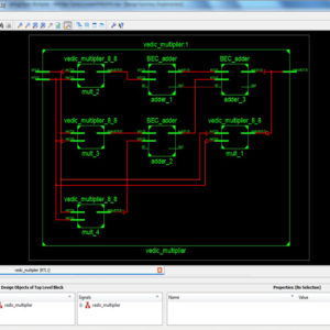
A Comparative Analysis of Multiplier Topologies using Different Vedic Sutras
Abstract: The need of low area and high speed Multiplier is increasing as the need of high speed processors are needed. The multipliers used in Square and cube architecture have to be more efficient in area and also in speed. In this paper a multiplier is implemented based on Nikhilam sutra with binary excess unit. The ripple carry adder in the multiplier architecture increases the speed of addition of partial products. The proposed architecture of this paper analysis the logic size, area and power consumption using Xilinx 14.2.
List of the following materials will be included with the Downloaded Backup: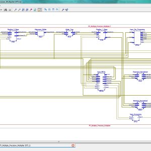
A Configurable Floating Point Multiple Precision Processing Element for HPC and AI Converged Computing
Abstract:
There is an emerging need to design configurable accelerators for the high-performance computing (HPC) and artificial intelligence (AI) applications in different precisions. Thus, the floating-point (FP) processing element (PE), which is the key basic unit of the accelerators, is necessary to meet multiple-precision requirements with energy-efficient operations. However, the existing structures by using high-precision-split (HPS) and low-precision-combination (LPC) methods result in low utilization rate of the multiplication array and long multi term processing period, respectively. In this article, a configurable FP multiple-precision PE design is proposed with the LPC structure. Half precision, single precision, and double precision are supported. The 100% multiplier utilization rate of the multiplication array for all precisions is achieved with improved speed in the comparison and summation process. The proposed design is realized in a 28-nm process with 1.429-GHz clock frequency. Compared with the existing multiple-precision FP methods, the proposed structure achieves 63% and 88% areasaving performance for FP16 and FP32 operations, respectively. The 4× and 20× maximum throughput rates are obtained when compared with fixed FP32 and FP64 operations. Compared with the previous multiple-precision PEs, the proposed one achieves the best energy-efficiency performance with 975.13 GFLOPS/W.
List of the following materials will be included with the Downloaded Backup: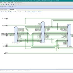
A Configurable Floating-Point Fused Multiply-Add Design with Mixed Precision for AI Accelerators
Base Paper Abstract:
Hardware accelerators for deep learning in artificial intelligence applications must often meet stringent constraints for accuracy and throughput. In addition to architecture/algorithm improvements, high performance computational techniques such as mixed precision are also required. In this paper, a floating-point (FP) fused multiply-add (FMA) unit supporting mixed/multiple precision is proposed. A wide range of conventional FP formats (such as half and single) as well as emerging formats (including E4M3, E5M2, DLFloat, BFLoat16 and TF32) are supported in the proposed design. In addition to all these formats, the proposed design is flexible in manipulating the exponent and mantissa lengths for 8, 16 and 32-bit FP numbers based on the needs of an application. The proposed FMA can be configured to support either multiple normal FMA operations, or alternatively mixed precision in ASIC. It is fully pipelined and in each cycle, the input bit streams are processed based on the provided configuration, so independent of the previous cycles. For normal FMA operations, the proposed design utilizes sharing of resources to parallelize multiple operations based on the available hardware and required precision. For mixed precision the FMA accumulates the lower precision dot products into higher precision to avoid overflow/underflow. It improves computational accuracy by adding all possible dot products at the same time while decreasing the number of rounding operations to prevent rounding errors. An innovative method to accumulate the dot products and the aligned addend is also proposed. By, considering tradeoffs between reusing the available hardware and removing unnecessary complex units, a more efficient and flexible design is attained in terms of hardware metrics and supported different precision computation compared to other designs found in the technical literature. Extensive simulation results for comparative analysis are provided.
List of the following materials will be included with the Downloaded Backup:
A Decoder for Short BCH Codes With High Decoding Efficiency and Low Power for Emerging Memories
Abstract:
In this paper, a double-error-correcting and triple error-detecting (DEC-TED) Bose–Chaudhuri–Hocquenghem (BCH) code decoder with high decoding efficiency and low power for error correction in emerging memories is presented. To increase the decoding efficiency, we propose an adaptive error correction technique for the DEC-TED BCH code that detects the number of errors in a codeword immediately after syndrome generation and applies a different error correction algorithm depending on the error conditions. With the adaptive error correction technique, the average decoding latency and power consumption are significantly reduced owing to the increased decoding efficiency. To further reduce the power consumption, an invalid-transition-inhibition technique is proposed to remove the invalid transitions caused by glitches of syndrome vectors in the error-finding block. Synthesis results with an industry-compatible 65-nm technology library show that the proposed decoders for the (79, 64, 6) BCH code take only 37%–48% average decoding latency and achieve more than 70% power reduction compared to the conventional fully parallel decoder under the 10−4–10−2 raw bit-error rate.
List of the following materials will be included with the Downloaded Backup:
A Design Implementation and Comparative Analysis of Advanced Encryption Standard (AES) Algorithm on FPGA
Abstract:
As the technology is getting advanced continuously the problem for the security of data is also increasing. The hackers are equipped with new advanced tools and techniques to break any security system. Therefore people are getting more concern about data security. The data security is achieved by either software or hardware implementations. In this work Field Programmable Gate Arrays (FPGA) device is used for hardware implementation since these devices are less complex, more flexible and provide more efficiency. This work focuses on the hardware execution of one of the security algorithms that is the Advanced Encryption Standard (AES) algorithm. The AES algorithm is executed on Vivado 2014.2 ISE Design Suite and the results are observed on 28 nanometers (nm) Artix-7 FPGA. This work discusses the design implementation of the AES algorithm and the resources consumed in implementing the AES design on Artix-7 FPGA. The resources which are consumed are as follows- Slice Register (SR), Look-Up Tables (LUTs), Input/Output (I/O) and Global Buffer (BUFG).
List of the following materials will be included with the Downloaded Backup: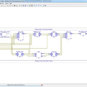
A Floating-Point Fused Dot-Product Unit
Abstract:
A floating-point fused dot-product unit is presented that performs single-precision floating-point multiplication and addition operations on two pairs of data in a time that is only 150% the time required for a conventional floating-point multiplication. When placed and routed in a 45nm process, the fused dot-product unit occupied about 70% of the area needed to implement a parallel dot-product unit using conventional floating-point adders and multipliers. The speed of the fused dot-product is 27% faster than the speed of the conventional parallel approach. The numerical result of the fused unit is more accurate because one rounding operation is needed versus at least three for other approaches.
List of the following materials will be included with the Downloaded Backup:
A High Speed CRC-32 Implementation on FPGA
Base Paper Abstract:
Cyclic Redundancy Check (CRC) is widely used for transmission error detection in various communication interfaces. As the transmission rate increases, accelerating CRC with lower resource consumption for high-speed interfaces becomes significant. This paper analyzes and implements a typical CRC algorithm (Stride-x) and designs a padding-zero strategy to support the input data length with multiples of byte. Besides, experiments are conducted to validate the proposed algorithm on Xilinx FPGA platforms. When stride is 1, the proposed algorithm outperforms a typical parallel CRC algorithm in throughput and resource consumption with various input bus widths (32/128/256 bits).
List of the following materials will be included with the Downloaded Backup:
A High-Performance Multiply-Accumulate Unit by Integrating Additions and Accumulations into Partial Product Reduction Process
Abstract:
In this paper, we propose a low-power high-speed pipeline multiply-accumulate (MAC) architecture. In a conventional MAC, carry propagations of additions (including additions in multiplications and additions in accumulations) often lead to large power consumption and large path delay. To resolve this problem, we integrate a part of additions into the pa rtial product reduction (PPR) process. In the proposed MAC architecture, the addition and accumulation of higher significance bits are not performed until the PPR process of the next multiplication. To correctly deal with the overflow in the PPR process, a small-size adder is designed to accumulate the total number of carries. Compared with previous works, experimental results show that the proposed MAC architecture can greatly reduce both power consumption and circuit area under the same timing constraint.
List of the following materials will be included with the Downloaded Backup:
A High-Throughput Hardware Accelerator for Lossless Compression of a DDR4 Command Trace
Abstract:
In a memory system, understanding how the host is stressing the memory is important to improve memory performance. Accordingly, the need for the analysis of memory command trace, which the memory controller sends to the dynamic random access memory, has increased. However, the size of this trace is very large; consequently, a high-throughput hardware (HW) accelerator that can efficiently compress these data in real time is required. This paper proposes a high throughput HW accelerator for lossless compression of the command trace. The proposed HW is designed in a pipeline structure to process Huffman tree generation, encoding, and stream merge. To avoid the HW cost increase owing to high throughput processing, a Huffman tree is efficiently implemented by utilizing static random access memory-based queues and bitmaps. In addition, variable length stream merge is performed at a very low cost by reducing the HW wire width using the mathematical properties of Huffman coding and processing the metadata and the Huffman codeword using FIFO separately. Furthermore, to improve the compression efficiency of the DDR4 memory command, the proposed design includes two preprocessing operations, the “don’t care bits override” and the “bits arrange,” which utilize the operating characteristics of DDR4 memory. The proposed compression architecture with such preprocessing operations achieves a high throughput of 8 GB/s with a compression ratio of 40.13% on average. Moreover, the total HW resource per throughput of the proposed architecture is superior to the previous implementations.
List of the following materials will be included with the Downloaded Backup: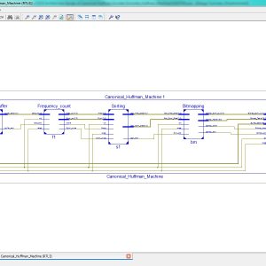
A High-Throughput VLSI Architecture Design of Canonical Huffman Encoder
Abstract:
In this brief, a high-throughput Huffman encoder VLSI architecture based on the Canonical Huffman method is proposed to improve the encoding throughput and decrease the encoding time required by the Huffman code word table construction process. We proposed parallel computing architectures for frequency-statistical sorting and code-size computational sorting. This architecture results in a process of building a tree and assigning symbols that can be completed by scanning the data only once. This solves the problem of the low efficiency of the traditional algorithm, which needs to scan the data twice. Consequently, in addition to the advantages of the high compression ratio inherited from the Canonical Huffman, the proposed architecture has overridden advantages for a high parallelism processing capacity. The experimental results showed that the proposed architecture decreased the encoding time by 26.30% compared to the available Huffman encoder using the standard algorithm when encoding 256 8-bit symbols. Furthermore, the VLSI architecture could further decrease the encoding time when encoding more 8-bit symbols. In particular, when encoding 212,642 8-bit symbols, the proposed VLSI architecture could reduce the encoding time by 87.40%. Thus, compared with the traditional Huffman encoders, this brief achieved the improvement of coding efficiency.
List of the following materials will be included with the Downloaded Backup: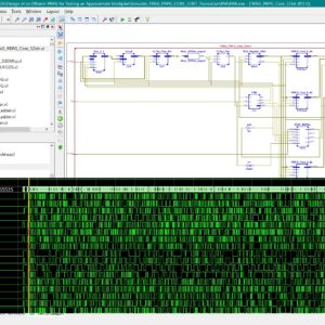
A Hybrid TRNG PRPG Architecture for Resource Efficient Static Segment and Truncation Multiplier
Reference Paper Abstract:
For error-tolerant applications, low power and small area can be achieved by approximation in calculation with acceptable loss of accuracy. Truncation of lower bits based on the number of significant digits is one of the techniques proposed for approximate multiplier. This paper proposes the area reduction of built-in self-test (BIST) circuitry for an approximate multiplier. The proposed pseudo random pattern generator (PRPG) provides test patterns to the multiplier such that truncation occurs evenly in the input numbers. The fault simulation results show that the proposed circuit can achieve higher fault coverage in the small area overhead required for PRPG. Index Terms: Design for Testability, BIST, PRPG, Approximate Computing, Multiplier
List of the following materials will be included with the Downloaded Backup: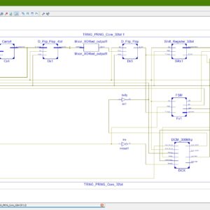
A Hybrid TRNG-PRNG Architecture for High-Performance and Resource-Efficient Random Number Generation on FPGA
Base Paper Abstract:
True random number generators (TRNGs) are fundamentals in many important security applications. Though they exploit randomness sources that are typical of the analog domain, digital-based solutions are strongly required especially when they have to be implemented on Field Programmable Gate Array (FPGA)-based digital systems. This paper describes a novel methodology to easily design a TRNG on FPGA devices. It exploits the runtime capability of the Digital Clock Manager (DCM) hardware primitives to tune the phase shift between two clock signals. The presented auto-tuning strategy automatically sets the phase difference of two clock signals in order to force on one or more flip-flops (FFs) to enter the metastability region, used as a randomness source. Moreover, a novel use of the fast carry-chain hardware primitive is proposed to further increase the randomness of the generated bits. Finally, an effective on-chip post-processing scheme that does not reduce the TRNG throughput is described. The proposed TRNG architecture has been implemented on the Xilinx Zynq XC7Z020 System on Chip (SoC). It passed all the National Institute of Standards and Technology (NIST) SP 800-22 statistical tests with a maximum throughput of 300×106 bit per second. The latter is considerably higher than the throughput of other previously published DCM based TRNGs.
List of the following materials will be included with the Downloaded Backup: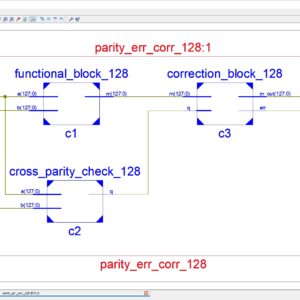
A Low-Complexity Multiple Error Correcting Architecture Using Novel Cross Parity Codes Over GF(2 m)
Abstract: This paper presents a modern low- complexity cross parity code, with a wide range of multiple bit error correction capability at a lower overhead, for improving the reliability. We have to use the two type of error correction technique for 128bit; first one is single bit error correction by using the hamming code. This hamming code is detects and then correct the single bit error correction. Another one is multiple bits error correction by using BCH (Bose–Choudhury– Hocquenghem). This one corrects the multiple bits error. Finally these are implemented and get the simulated result is compared to the previous architecture. The code are simulated and power, area, cost are taken using Xilinx 14.2 software.
List of the following materials will be included with the Downloaded Backup:
A Novel Design of Flip-Flop Circuits using Quantum Dot Cellular Automata (QCA)
Abstract:
As the device dimension is shrinking day by day the conventional transistor based CMOS technology encounters serious hindrances due to the physical barriers of the technology such as ultra-thin gate oxides, short channel effects, leakage currents & excessive power dissipation at nano scale regimes. Quantum Dot Cellular Automata is an alternate challenging quantum phenomenon that provides a completely different computational platform to design digital logic circuits using quantum dots confined in the potential well to effectively process and transfer information at nano level as a competitor of traditional CMOS based technology. This paper has demonstrated the implementation of circuits like D, T and JK flip flops using a derived expression from SR flip-flop. The kink energy and energy dissipations has been calculated to determine the robustness of the designed flip-flops. The simulation results have been verified using QCA Designer simulation tool.
List of the following materials will be included with the Downloaded Backup:
A Novel Design of High Speed Multiplier Using Hybrid Adder Technique
Base Paper Abstract:
Electronic devices are necessary in small spaces in order to provide fast speed and low power consumption. Arithmetic operations determine how quickly electronics operate. In many applications involving VLSI signal processing, multiplication is a necessary arithmetic operation. Thus, to create any kind of signal processing module, a high-speed multiplier is a prerequisite. Every individual has different needs and goals, which has led to the development of different multipliers according to the need of application. In this paper, a Hybrid multiplier is proposed and designed using hybrid adders which is a mixture of Brent Kung adder and Kogge Stone adder which results in less delay i.e. 4.062ns compared to other multipliers existed.
List of the following materials will be included with the Downloaded Backup:
A Novel In-Memory Wallace Tree Multiplier Architecture Using Majority Logic
Abstract:
In-memory computing using emerging technologies such as resistive random-access memory (ReRAM) addresses the ‘von Neumann bottleneck’ and strengthens the present research impetus to overcome the memory wall. While many methods have been recently proposed to implement Boolean logic in memory, the latency of arithmetic circuits (adders and consequently multipliers) implemented as a sequence of such Boolean operations increases greatly with bit-width. Existing in-memory multipliers require O(n2) cycles which is inefficient both in terms of latency and energy. In this work, we tackle this exorbitant latency by adopting Wallace Tree multiplier architecture and optimizing the addition operation in each phase of the Wallace Tree. Majority logic primitive was used for addition since it is better than NAND/NOR/IMPLY primitives. Furthermore, high degree of gate-level parallelism is employed at the array level by executing multiple majority gates in the columns of the array. In this manner, an in-memory multiplier of O(n.log(n)) latency is achieved which outperforms all reported in-memory multipliers. Furthermore, the proposed multiplier can be implemented in a regular transistor-accessed memory array without any major modifications to its peripheral circuitry and is also energy-efficient.
List of the following materials will be included with the Downloaded Backup: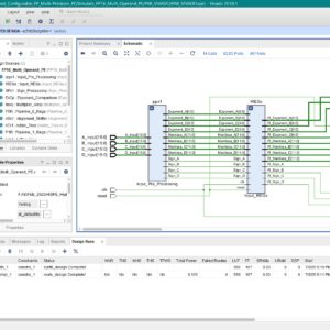
A Pipelined Fused Multiply-Add Architecture for Configurable FP16 Multi-Operand Operations
Base Paper Abstract:
Multiple precision modes are needed for a floating-point processing element (PE) because they provide flexibility in handling different types of numerical data with varying levels of precision and performance metrics. Performing high-precision floating-point operations has the benefits of producing highly precise and accurate results while allowing for a greater range of numerical representation. Conversely, low-precision operations offer faster computation speeds and lower power consumption. In this paper, we propose a configurable multi-precision processing element (PE) which supports Half Precision, Single Precision, Double Precision, BrainFloat-16 (BF-16) and TensorFloat-32 (TF-32). The design is realized using GPDK 45 nm technology and operated at 281.9 MHz clock frequency. The design was also implemented on Xilinx ZCU104 FPGA evaluation board. Compared with previous state-of-the-art (SOTA) multiprecision PEs, the proposed design supports two more floating point data formats namely BF-16 and TF-32. It achieves the best energy performance with 2368.91 GFLOPS/W and offers 63% improvement in operating
List of the following materials will be included with the Downloaded Backup:
A Reversible Processor Architecture and Its Reversible Logic Design
Proposed Abstract:
This paper presents the design and FPGA implementation of a 16-bit reversible processor architecture employing Fredkin, Feynman, and PERES gate architectures for reversible logic design. Reversible computing offers promising advantages in terms of energy efficiency and information loss prevention, making it suitable for various emerging computing paradigms. The proposed processor architecture encompasses a carefully crafted instruction set, data path, and control logic, all realized using reversible logic gates. Key components such as the ALU, register file, and memory elements are designed with an emphasis on reversibility. The design is implemented using Hardware Description Languages (HDLs), targeting a specific FPGA platform. The paper outlines the design methodology, gate-level implementation details, memory design considerations, FPGA synthesis, and testing procedures. Furthermore, it discusses optimization strategies and presents simulation results to validate the functionality and efficiency of the proposed reversible processor architecture. This work contributes to the advancement of reversible computing and provides insights into the practical realization of reversible processor architectures on FPGA platforms.
List of the following materials will be included with the Downloaded Backup:
A Review on Fundamentals of Ternary Reversible Logic Circuits
Abstract:
One of the main motivations for using ternary logic systems is the amount of information per circuit line is higher as compared to the corresponding binary logic representation, thereby leading to more compact circuit realizations. This is particularly attractive for quantum computing as quarts are expensive resources and minimizing their number is one of the main objectives during synthesis. Therefore, ternary reversible logic synthesis has drawn significant attention among researchers. It deals with fundamental unit of information called quarts that can exist in one of the three states |0, |1 and |2. Hence, the aim of this paper is to bridge the knowledge gap for the beginners in this domain than searching the entire space. Therefore, the present work discusses the basic concepts of ternary reversible logic and ternary reversible gates. The detailed discussion of the various ternary reversible logic synthesis will enable the beginners in this domain to understand the ternary reversible logic in a better way.
List of the following materials will be included with the Downloaded Backup: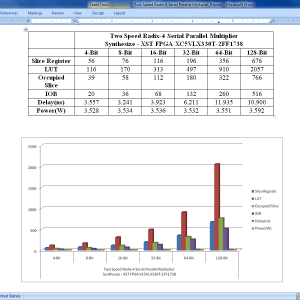
A Two-Speed, Radix-4, Serial–Parallel Multiplier (Booth Multiplier )
Abstract:
In this paper, we present a two-speed, radix-4, serial-parallel multiplier for accelerating applications such as digital filters, artificial neural networks, and other machine learning algorithms. Our multiplier is a variant of the serial–parallel (SP) modified radix-4 Booth multiplier that adds only the nonzero Booth encodings and skips over the zero operations, making the latency dependent on the multiplier value. Two sub circuits with different critical paths are utilized so that throughput and latency are improved for a subset of multiplier values. The multiplier is evaluated on an Intel Cyclone V field-programmable gate array against standard parallel–parallel and SP multipliers across four different process–voltage–temperature corners. We show that for bit widths of 32 and 64, our optimizations can result in a 1.42×–3.36× improvement over the standard parallel Booth multiplier in terms of area–time depending on the input set.
List of the following materials will be included with the Downloaded Backup:
A Unified Approach for Realization of IIR Filters in Delta Domain
Base Paper Abstract:
In this paper, digital realization of IIR filters is concentrated in discrete delta domain. Whenever, a continuous time filter is discretized at fast sampling rate, corresponding discrete time filter in conventional z-domain realization fails to provide meaningful information. In other way, the delta domain based system provides the continuous time results at fast sampling rate leading to the development of a unified method for filter realization in digital domain. Realization of the digital filter using delta operator is having very good finite word length performance under high sampling rate. Three different types of IIR filters are considered for the digital realization in delta domain. The transposed delta direct form II (DDFT-II) structure is used to realize the filters, as it is the most suitable structure for digital filter realization. Butterworth, Chebyshev -2 and Elliptic filters are considered as example and MATLAB Simulink is used to realize the digital filter in delta domain. The frequency
List of the following materials will be included with the Downloaded Backup:
Advanced Encryption Standard Algorithm with Optimal S-box and Automated Key Generation
Base Paper Abstract:
Advanced Encryption Standard (AES) algorithm plays an important role in a data security application. In general S-box module in AES will give maximum confusion and diffusion measures during AES encryption and cause significant path delay overhead. In most cases, either LUTs or embedded memories are used for S- box computations which are vulnerable to attacks that pose a serious risk to real-world applications. In this paper, implementation of the composite field arithmetic-based Sub-bytes and inverse Sub-bytes operations in AES is done. The proposed work includes an efficient multiple round AES cryptosystem with higher-order transformation and composite field s-box formulation with some possible inner stage pipelining schemes which can be used for throughput rate enhancement along with path delay optimization. Finally, input biometric-driven key generation schemes are used for formulating the cipher key dynamically, which provides a higher degree of security for the computing devices.
List of the following materials will be included with the Downloaded Backup:
Algorithm Level Error Detection in Low Voltage Systolic Array
Base Paper Abstract:
In this brief an approach is proposed to achieve energy savings from reduced voltage operation. The solution detects timing-errors by integrating Algorithm Based Fault Tolerance (ABFT) into a digital architecture. The approach has been studied with a systolic array matrix multiplier operating at reduced voltages, detecting errors on-the-fly to avoid energy demanding memory round-trips. The analysis of the solution has been done using analog-digital co-simulation to extract the transient behavior under different voltages and clock frequencies. HSPICE simulations using 90nm CMOS transistor models, and experiments by reducing operation voltage of an FPGA device were carried out. HSPICE simulations, showed possibility of 10x increase in energy-efficiency by approaching near-threshold region.
List of the following materials will be included with the Downloaded Backup:
An Efficient and High Speed Overlap Free Karatsuba Based Finite Field Multiplier for FPGA Implementation
Abstract:
Cryptography systems have become inseparable parts of almost every communication device. Among cryptography algorithms, public-key cryptography, and in particular elliptic curve cryptography (ECC), has become the most dominant protocol at this time. In ECC systems, polynomial multiplication is considered to be the most slow and area consuming operation. This article proposes a novel hardware architecture for efficient field-programmable gate array (FPGA) implementation of Finite field multipliers for ECC. Proposed hardware was implemented on different FPGA devices for various operand sizes, and performance parameters were determined. Comparing to state-of-the art works, the proposed method resulted in a lower combinational delay and area–delay product indicating the efficiency of design.
List of the following materials will be included with the Downloaded Backup:
An Efficient Approximate Sum of Absolute Differences Hardware for FPGAs
Proposed Abstract:
Sum of Absolute Differences (SAD) is mainly applied in block-matching tasks such as motion estimation for video compression, stereo matching for depth/disparity calculation, template matching in image/object detection, image registration (including medical imaging), and lightweight optical-flow/tracking systems, because it is simple, fast, and hardware-friendly. The Traditional accurate SAD hardware provides exact results but consumes high power and requires large area, while existing approximate designs reduce cost but often suffer from high errors and poor FPGA-specific optimization. To overcome these limitations, this work proposes an improved SAD hardware architecture that replaces the conventional full adder with a lightweight XOR–MUX structure. This change reduces delay, minimizes area, and increases speed by removing redundant logic and optimizing FPGA resource utilization. The novelty of the design lies in combining approximation with FPGA-aware optimization, achieving bounded error, reduced power consumption, and higher operating frequency. The proposed system is implemented in Verilog HDL and tested on a Xilinx FPGA, showing improvements in LUT usage, clock frequency, and power efficiency, making it suitable for real-time video and image processing applications.
List of the following materials will be included with the Downloaded Backup:
An Efficient Constant Multiplier Architecture Based on Vertical-Horizontal Binary Common Sub-expression Elimination Algorithm for Reconfigurable FIR Filter Synthesis.
Abstract: This paper proposes efficient constant multiplier architecture based on vertical-horizontal binary common sub-expression elimination (VHBCSE) algorithm for designing a reconfigurable finite impulse response (FIR) filter whose coefficients can dynamically change in real time. To design an efficient reconfigurable FIR filter, according to the proposed VHBCSE algorithm, 2-bit binary common sub-expression elimination (BCSE) algorithm has been applied vertically across adjacent coefficients on the 2-D space of the coefficient matrix initially, followed by applying variable-bit BCSE algorithm horizontally within each coefficient. Faithfully rounded truncated multiple constant multiplication/accumulation (MCMAT) and multi-root binary partition graph (MBPG) respectively. Efficiency shown by the results of comparing the FPGA and ASIC implementations of the reconfigurable FIR filter designed using VHBCSE algorithm based constant multiplier establishes the suitability of the proposed algorithm for efficient fixed point reconfigurable FIR filter synthesis.
List of the following materials will be included with the Downloaded Backup: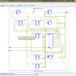
An Efficient Design for Reversible Wallace Unsigned Multiplier
Abstract:
Today, reversible logic can be used for designing low-power CMOS circuits, optical data processing, DNA computations, biological researches, quantum circuits and nanotechnology. Sometimes using of reversible logic is inevitable such as build quantum computers. Reversible logic circuits structure is much more complicated than irreversible logic circuits. Multiplication operation is considered as one of the most important operations in the ALU unit. In this paper, we have proposed two 4×4 reversible unsigned multiplier circuits in which Wallace tree method is used to reduce the depth of circuits. In first design, the partial products circuit is designed using TG and FG gates so that TG is used to produce the partial products and FG for fan-out. In the second design, TG and PG gates are used to produce the partial products and no fan-out is required. Moreover, we have used PG gate and Feynman' block as reversible half-adder (HA) and full-adder (FA) in the summation network, respectively. In the first design, the main purpose is to decrease the depth of the circuit and increase the circuit speed. In the second design we would attempt to improve quantum parameters the number of garbage outputs, constant inputs and quantum cost. The evaluation results show that the first design, in terms of delay, is the fastest circuit. Also, the second design in terms of the number of constant inputs, garbage outputs and quantum cost is better than other designs.
List of the following materials will be included with the Downloaded Backup: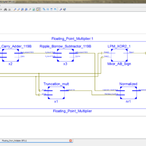
An Efficient Implementation of Floating Point Multiplier
Abstract:
In this paper we describe an efficient implementation of an IEEE 754 single precision floating point multiplier targeted for Xilinx Virtex-5 FPGA. VHDL is used to implement a technology-independent pipelined design. The multiplier implementation handles the overflow and underflow cases. Rounding is not implemented to give more precision when using the multiplier in a Multiply and Accumulate (MAC) unit. With latency of three clock cycles the design achieves 301 MFLOPs. The multiplier was verified against Xilinx floating point multiplier core.
List of the following materials will be included with the Downloaded Backup:
An LUT Based RNS FIR Filter Implementation for Reconfigurable Applications
Abstract:
In this work, two approaches to realize a look up table (LUT) based finite impulse response (FIR) filter using Residue Number System (RNS) are proposed. The proposed implementations take advantage of shift and add approach offered by the chosen module set. The two proposed filter architecture are compared with an earlier proposed version of reconfigurable RNS FIR filter. The filters are synthesized using Cadence RTL compiler in UMC 90 nm technology. The performance of the filters are compared in terms of Area (A), Power (P), and Delay (T). The results show that one of the proposed architecture offers significant improvement in terms of delay, while the second approach is well suited for applications that require minimal power and area. Both implementations offer advantage in area delay and power-delay-product. Proposed approaches are also verified functionally using Altera DSP Builder.
List of the following materials will be included with the Downloaded Backup: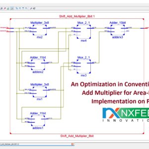
An Optimization in Conventional Shift &Add Multiplier for Area-Efficient Implementation on FPGA
Base Paper Abstract:
FPGA is familiar with prototyping and implementing simple to complex DSP systems. The FPGA based design may be highly affected by factors that include selection of an FPGA board, Electronic Design Automation Tool and the Programming Techniques to optimize the algorithm. The algorithm optimization results in a more compact design regarding the area and achieved frequency. In DSP algorithms optimization, the major bottleneck is the multiplier complexity evident in, for example - FIR, IIR, FFT, and others. Research shows much work on multiplier optimization. Despite all possible optimization techniques, the multiplier consumes tremendous resources when translated on hardware, with more power consumption and observed delay. The proposed work is novel in that it brings resources optimization in a familiar shift and add multiplier algorithm by implementing the design in FPGA and comparing the results with the existing shift, and add a multiplier. In the implementation of the design, Xilinx Vertex -7 FPGA is used along with ISE 14.2 simulators. The parameters to compare are the Lookup tables (Logic element of FPGA), adder/subtractors and the multiplexers, along with performance characters, like the operating frequency, delay and total levels of logic (path travelled by the signal in register transfer level). The output shows that the anticipated design is an excellent alternative to the conventional shift and add algorithm.
List of the following materials will be included with the Downloaded Backup: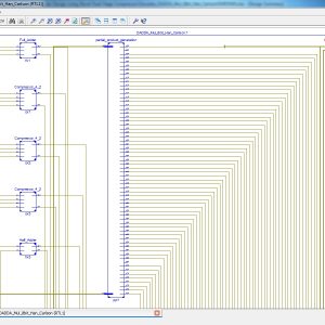
Approximate Multiplier Design Using Novel Dual-Stage 4 : 2 Compressors
Base Paper Abstract:
High speed multimedia applications have paved way for a whole new area in high speed error-tolerant circuits with approximate computing. These applications deliver high performance at the cost of reduction in accuracy. Furthermore, such implementations reduce the complexity of the system architecture, delay and power consumption. This paper explores and proposes the design and analysis of two approximate compressors with reduced area, delay and power with comparable accuracy when compared with the existing architectures. The proposed designs are implemented using 45 nm CMOS technology and efficiency of the proposed designs have been extensively verified and projected on scales of area, delay, power, Power Delay Product (PDP), Error Rate (ER), Error Distance (ED), and Accurate Output Count (AOC). The proposed approximate 4 : 2 compressor shows 56.80% reduction in area, 57.20% reduction in power, and 73.30% reduction in delay compared to an accurate 4 : 2 compressor. The proposed compressors are utilised to implement 8 × 8 and 16 × 16 Dadda multipliers. These multipliers have comparable accuracy when compared with state-of-the-art approximate multipliers. The analysis is further extended to project the application of the proposed design in error resilient applications like image smoothing and multiplication.
List of the following materials will be included with the Downloaded Backup: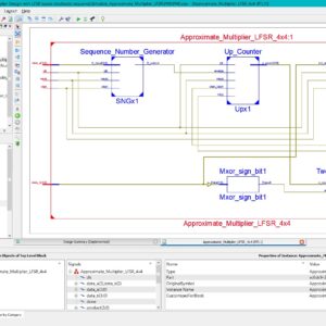
Approximate Multiplier Design with LFSR-Based Stochastic Sequence Generators for Edge AI
Base Paper Abstract:
This letter introduces an innovative approximate multiplier (AM) architecture that leverages stochastically generated bit streams through the Linear Feedback Shift Register (LFSR). The AM is applied to matrix-vector multiplication (MVM) in Neural Networks (NNs). The hardware implementations in 90 nm CMOS technology demonstrate superior power and area efficiency compared to state-of-the-art designs. Additionally, the study explores applying stochastic computing to LSTM NNs, showcasing improved energy efficiency and speed.
List of the following materials will be included with the Downloaded Backup:
Area Delay and Energy Efficient Multi-Operand Binary Tree Adder
Abstract:
Here, the critical path of ripple carry adder (RCA)-based binary tree adder (BTA) is analyzed to find the possibilities for delay minimization. Based on the findings of the analysis, the new logic formulation and the corresponding design of RCA are proposed for the BTA. The comparison result shows that the proposed RCA design offers better efficiency in terms of area, delay and energy than the existing RCA. Using this RCA design, the BTA structure is proposed. The synthesis result reveals that the proposed 32-operand BTA provides the saving of 22.5% in area–delay product and 28.7% in energy–delay product over the recent Wallace tree adder which is the best among available multi-operand adders. The authors have also applied the proposed BTA in the recent multiplier designs to evaluate its performance. The synthesis result shows that the performance of multiplier designs improved significantly due to the use of proposed BTA. Therefore, the proposed BTA design can be a better choice to develop the area, delay and energy efficient digital systems for signal and image processing applications.
List of the following materials will be included with the Downloaded Backup: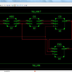
Area Delay Power Efficient Carry Select Adder
Source : VHDL
Abstract:
We are briefly discussing the logic operations are involved in the CSLA (conventional carry select adder) and the square root conventional carry select adder. We have discard the all the extra logic operations present in the conventional CSLA. In the proposed system carry selection is take place in before the final sum calculation. The proposed system achieves the optimization in the logic units. Finally the FPGA synthesis results shows to achieves a design the low power architecture for CSLA.
List of the following materials will be included with the Downloaded Backup:
Area-Efficient Bidirectional Shift-Register Using Bidirectional Pulsed-Latches
Abstract:
This paper proposes an area-efficient bidirectional shift-register using bidirectional pulsed-latches. The proposed bidirectional shift-register reduces the area and power consumption by replacing master-slave flip-flops and 2-to-1 multiplexers with the proposed bidirectional pulsed-latches and non-overlap delayed pulsed clock signals, and by using sub shift-registers and extra temporary storage latches. A 256-bit bidirectional shift-register was fabricated using a 65nm CMOS process. Its area was 1,943μm2 and its power consumption is 200μW at a 100MHz clock frequency with VDD=1.2V. It reduces area by 39.2% and power consumption by 19.4% compared to the conventional bidirectional shift-register, length in most cases.
List of the following materials will be included with the Downloaded Backup:
ASIC design of UHF RFID reader digital baseband
This paper presents the ASIC design and implementation of digital baseband system for UHF RFID reader based on EPC Global C1G2 /ISO 18000-6c protocol. The digital baseband system consists of two parts :transmitter and receiver, which including encoding module, decoding module, channel filers, CRC check module, control module and a SPI module. It is described in verilog HDL in RTL level, with Design Complier for synthesizing, PT for static timing analyzing and Astro for physical design. The die is fabricated using IBM 130nm 8-layer-metal RF CMOS process successfully, which size is 3 mm x 3mm, the power consumption is around 6.7mW. It can be applied in the research of single-chip UHF RFID reader. The proposed architecture of this paper analysis the logic size, area and power consumption using Xilinx 14.2.
List of the following materials will be included with the Downloaded Backup:
AxPPA: Approximate Parallel Prefix Adders
Base Paper Abstract:
Addition units are widely used in many computational kernels of several error-tolerant applications such as machine learning and signal, image, and video processing. Besides their use as stand-alone, additions are essential building blocks for other math operations such as subtraction, comparison, multiplication, squaring, and division. The parallel prefix adders (PPAs) is among the fastest adders. It represents a parallel prefix graph consisting of the carry operator nodes, called prefix operators (POs). The PPAs, in particular, are among the fastest adders because they optimize the parallelization of the carry generation (G) and propagation (P). In this work, we introduce approximate PPAs (AxPPAs) by exploiting approximations in the POs. To evaluate our proposal for approximate POs (AxPOs), we generate the following AxPPAs, consisting of a set of four PPAs: approximate Brent–Kung (AxPPA-BK), approximate Kogge–Stone (AxPPAKS), Ladner-Fischer (AxPPA-LF), and Sklansky (AxPPA-SK). We compare four AxPPA architectures with energy-efficient approximate adders (AxAs) [i.e., Copy, error-tolerant adder I (ETAI), lower-part OR adder (LOA), and Truncation (trunc)]. We tested them generically in stand-alone cases and embedded them in two important signal processing application kernels: a sum of squared differences (SSDs) video accelerator and a finite impulse response (FIR) filter kernel. The AxPPA-LF provides a new Pareto front in both energy-quality and area-quality results compared to state-of-the-art energy-efficient AxAs.
List of the following materials will be included with the Downloaded Backup:
Byte-Reconfigurable LDPC Codec Design With Application to High-Performance ECC of NAND Flash Memory Systems
Abstract: In information theory, a low-density parity-check (LDPC) code is a linear error correcting code, a method of transmitting a message over a noisy transmission channel. An LDPC is constructed using a sparse bipartite graph. LDPC codes are capacity-approaching codes, which means that practical constructions exist that allow the noise threshold to be set very close (or even arbitrarily close on the BEC) to the theoretical maximum (the Shannon limit) for a symmetric memory-less channel. The noise threshold defines an upper bound for the channel noise, up to which the probability of lost information can be made as small as desired. Using iterative belief propagation techniques, LDPC codes can be decoded in time linear to their block length.
List of the following materials will be included with the Downloaded Backup:
Combating Data Leakage Trojans in Commercial and ASIC Applications With Time-Division Multiplexing and Random Encoding
Proposed Abstract:
This paper explains the concept of reduction of data leakage Trajons in modulation scheme of TDM (Time Division Multiplexing) using DES (Data Encryption Standard) encoding and decoding concept. The DES is a symmetric key block cipher which is used for encryption and decryption process. In hardware manufacturing, detection and prevention of hardware Trajons attacks becomes a major concern for a manufacturing company. Because, the hardware Trajons is able to steal some sensitive information of a users such as encryption keys, passwords, etc,. So, most defensive methods prefers on prevention of data. The existing system uses the concept of RECORD ( Randomized encoding of combinational logic for resistance to data leakage) to prevent the data from the hardware Trajons even the Trajons known the entire information. Thus the proposed system of TDM version of RECORD design is more secure than the Sequential RECORD system and these case of existing work, will not concentrate and proved TDM RECORD DES Decryption Algorithm. Therefore, the proposed work of this paper will used the concept of TDM version using RECORD with implement in Encryption and Decryption Algorithm and also BER Testing, this method will have designed in Verilog HDL and implement in Xilinx FPGA and finally shown the comparison results in terms of area, delay and power.
List of the following materials will be included with the Downloaded Backup:
Comparative study of 16-order FIR filter design using different multiplication techniques
Abstract:
This study represents designing and implementation of a low power and high speed 16 order FIR filter. To optimize filter area, delay and power, different multiplication techniques such as Vedic multiplier, add and shift method and Wallace tree (WT) multiplier are used for the multiplication of filter coefficient with filter input. Various adders such as ripple carry adder, Kogge Stone adder, Brent Kung adder, Ladner Fischer adder and Han Carlson adder are analyzed for optimum performance study for further use in various multiplication techniques along with barrel shifter. Secondly optimization of filter area and delay is done by using add and shift method for multiplication, although it increases power dissipation of the filter. To reduce the complexity of filter, coefficients are represented in canonical signed digit representation as it is more efficient than traditional binary representation. The finite impulse-response (FIR) filter is designed in MATLAB using equiripple method and the same filter is synthesized on Xilinx Spartan 3E XC3S500E target field-programmable gate array device using Very High Speed Integrated Circuit Hardware Description Language (VHDL) subsequently the total on-chip power is calculated in Vivado2014.4. The comparison of simulation results of all the filters show that FIR filter with WT multiplier is the best optimized filter.
List of the following materials will be included with the Downloaded Backup:
Comparison and Extension of Approximate 4-2 Compressors for Low-Power Approximate Multipliers
Abstract:
Approximate multipliers attract a large interest in the scientific literature that proposes several circuits built with approximate 4-2 compressors. Due to the large number of proposed solutions, the designer who wishes to use an approximate 4-2 compressor is faced with the problem of selecting the right topology. In this paper, we present a comprehensive survey and comparison of approximate 4-2 compressors previously proposed in literature. We present also a novel approximate compressor, so that a total of twelve different approximate 4-2 compressors are analyzed. The investigated circuits are employed to design 8 × 8 and 16 × 16 multipliers, implemented in 28nm CMOS technology. For each operand size we analyze two multiplier configurations, with different levels of approximations, both signed and unsigned. Our study highlights that there is no unique winning approximate compressor topology since the best solution depends on the required precision, on the signedness of the multiplier and on the considered error metric.
List of the following materials will be included with the Downloaded Backup:
Concept Design and Implementation of Reconfigurable CORDIC
This brief presents the key concept, design strategy, and implementation of reconfigurable coordinate rotation digital computer (CORDIC) architectures that can be configured to operate either for circular or for hyperbolic trajectories in rotation as well as vectoring-modes. It can, therefore, be used to perform all the functions of both circular and hyperbolic CORDIC. We propose three reconfigurable CORDIC designs: 1) a reconfigurable rotation-mode CORDIC that operates either for circular or for hyperbolic trajectory; 2) a reconfigurable vectoring-mode CORDIC for circular and hyperbolic trajectories; and 3) a generalized reconfigurable CORDIC that can operate in any of the modes for both circular and hyperbolic trajectories. The reconfigurable CORDIC can perform the computation of various trigonometric and exponential functions, logarithms, square-root, and so on of circular and hyperbolic CORDIC using either rotation-mode or vectoring-mode CORDIC in one single circuit. It can be used in digital synchronizers, graphics processors, scientific calculators, and so on. It offers substantial saving of area complexity over the conventional design for reconfigurable applications. The proposed architecture of this paper analysis the logic size, area and power consumption using Xilinx 14.2.
List of the following materials will be included with the Downloaded Backup:
Design and Analysis of a Majority Logic Based Imprecise 6-2 Compressor for Approximate Multipliers
Base Paper Abstract:
Approximate computing is an emerging paradigm for trading off computing accuracy to reduce energy consumption and design complexity in a variety of applications, for which exact computation is not a critical requirement. Different from conventional designs using AND-OR and XOR gates, the majority gate is widely used in many emerging nanotechnologies. An ultra-efficient 6-2 compressor is proposed in this paper. It is composed of two majority gates that lead to low energy consumption and high hardware efficiency. The proposed compressor is utilized in the approximate partial product reduction of a modified 8×8 Dadda multiplier with a truncated structure. Experimental results show that this multiplier realizes a significant reduction in hardware cost, especially in terms of power and area, on average by up to 40% and 31% respectively, compared to exact and state-of-the-art designs. The application of image multiplication is also presented to assess the practicability of the multiplier. The results show that the proposed multiplier results in images with higher quality in peak signal to noise ratio (PSNR) and mean structural similarity index metric (MSSIM) compared to other designs.
List of the following materials will be included with the Downloaded Backup: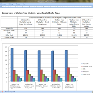
Design and analysis of High speed Wallace tree multiplier using parallel prefix adders for VLSI circuit designs
Abstract:
Major operation block in any processing unit is a multiplier. There are many multiplication algorithms are proposed, by using which multiplier structure can be designed. Among various multiplication algorithms, Wallace tree multiplication algorithm is beneficial in terms of speed of operation. With the advancement of technology, demand for circuits with high speed and low area is increasing. In order to improve the speed of Wallace tree multiplier without degrading its area parameter, a new structure of Wallace tree multiplier is proposed in this paper. In the proposed structure, the final addition stage of partial products is performed by parallel prefix adders (PPAs). In this paper, five Wallace tree multiplier structures are proposed using Kogge stone adder, Sklansky adder, Brent Kung adder, Ladner Fischer adder and Han carlson adder. All the multiplier structures are designed using Verilog HDL in Xilinix 13.2 design suite. The proposed structures are simulated using ISIM simulator and synthesized using XST synthesizer. The proposed designs are analyzed with respect to traditional multiplier design in terms of area (No. of LUTs) and delay (ns).
List of the following materials will be included with the Downloaded Backup: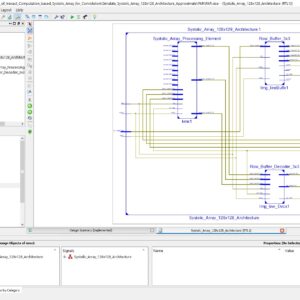
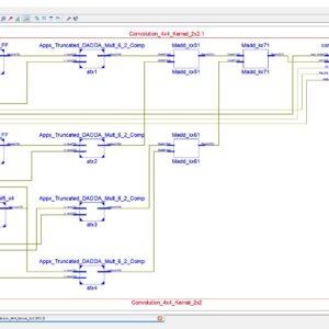
Design and Evaluation of Inexact Computation based Systolic Array for Convolution
Base Paper Abstract:
Systolic Array (SA) architecture is a unique computation architecture where the inputs are continuously flowing, and the processing elements perform the desired computations in parallel. SA’s are prominently investigated due to the emergence of heavy and large processing elements for modern-day Convolution Neural Network (CNN) applications. Taking this cue, SA architectures of the order of kernel size and configured with approximate multipliers are investigated for image processing applications. The approximate array multiplier derived from approximate 4-2 compressors were employed to achieve hardware benefits without losing on the image quality metrics. The SA architecture is configured to the same size as filter kernels in a view to achieve maximum utilization, and the same is compared with other existing SA architectures for hardware metrics. The computational time for processing an image of size 256 × 256 was evaluated for approximated SA. This work investigates approximate SA for Gaussian smoothing and image outline feature extraction applications to showcase the reliability of the design. The novel approximate SA architecture is a step toward designing compact sized SoC designs for real-time image and video processing applications.
List of the following materials will be included with the Downloaded Backup:
Design and Implementation of 32-bit CSPRNG using the PRESENT cipher with Dual Polynomial PRNG for Enhanced Randomness and Precision
Base Paper Abstract:
Random Number Generators (RNGs) are substantially used in many security domains, providing a fundamental source of unpredictability essential for tasks such as cryptography, simulations, and statistical analyses. The efficiency and quality of an RNG directly impact the reliability and security of diverse applications, making advancements in RNG design, as explored in this study, of significant importance for enhancing computational processes. This paper presents an innovative Pseudo-Random Number Generator (PRNG) that leverages the efficiency of two carefully selected Linear Feedback Shift Registers (LFSRs) and a connecting XOR gate. The investigation of five polynomials identified an optimal pair, resulting in a notable improvement of over 200X in the length of random bit sequences compared to a single LFSR-based PRNG. The Basys3 FPGA board with the xc7a35tcpg236-1 FPGA chip was used to implement and synthesize the proposed design. Two significant findings emerge from this research. Firstly, using variable polynomials demonstrates a huge enhancement in the duration of randomness, outperforming the impact of variable seeds. A noteworthy observation is that employing the same polynomials in different branches does not result in optimal results. Secondly, managing more seeds is associated with an increased area cost, underscoring the efficiency of handling two polynomials.
List of the following materials will be included with the Downloaded Backup:
Design and Implementation of a Unified Digital Clock and Stopwatch System Using FSM and Multiplexed Seven-Segment Display
Proposed Abstract:
Digital clocks and stopwatches are widely used in daily applications such as consumer electronics, embedded devices, portable medical instruments, and time monitoring systems, as they provide simple and accurate time tracking functions. These systems offer advantages like low cost, user-friendly operation, and high reliability; however, they often face disadvantages such as hardware redundancy, higher power consumption, and limited integration when clock and stopwatch functions are implemented separately. The main problem addressed in this work is the lack of a unified architecture that can perform both digital clock and stopwatch operations using shared resources, which leads to inefficient hardware utilization and increased complexity in existing designs. Conventional systems generally use independent controllers and dedicated display drivers, resulting in additional overhead. To overcome this limitation, we propose a finite state machine based architecture that integrates both digital clock and stopwatch modules into a single design with common display hardware. The system employs multiplexers and control signals to switch seamlessly between clock and stopwatch modes, while states such as idle, hour, minute, second, and pause are clearly managed through FSM logic. The novelty of this work lies in the resource-sharing approach where a common seven-segment display is driven by multiplexed outputs, thereby reducing area, power, and switching complexity without compromising accuracy. The proposed design is implemented and tested using hardware description language coding and simulated on FPGA-based platforms, ensuring precise timing, functional correctness, and display reliability. Performance evaluation confirms that the system achieves efficient utilization of logic resources, accurate real-time operation, and flexibility for future extension in low-power VLSI and IoT-based applications.
List of the following materials will be included with the Downloaded Backup:
Design and Implementation of an 8-bit Approximate Wallace Tree Multiplier for Energy Efficient Deep Neural Networks
Base Paper Abstract:
Approximate arithmetic computing circuits and architectures have been proven to be energy efficient designs for Deep Neural Networks (DNNs) which are error resilient. In this paper, an approximate 8-bit Wallace Multiplier has been proposed and designed in 90nm CMOS technology for energy efficiency. The proposed 8-bit approximate multiplier design consumes ~32% less energy in comparison to an accurate 8-bit Wallace Tree multiplier with less than 20% Mean Relative Error (MRE).
List of the following materials will be included with the Downloaded Backup:
Design and Low-Complexity Implementation of Matrix–Vector Multiplier for Iterative Methods in Communication Systems
Abstract: Iterative methods are basic building blocks of communication systems and often represent a dominating part of the system, and therefore, they necessitate careful design and implementation for optimal performance. In this brief, we propose a novel field programmable gate arrays design of matrix–vector multiplier that can be used to efficiently implement widely adopted iterative methods. The proposed design exploits the sparse structure of the matrix as well as the fact that spreading code matrices have equal magnitude entries. Implementation details and timing analysis results are promising and are shown to satisfy most modern communication system requirements.
List of the following materials will be included with the Downloaded Backup: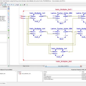
Design of High Speed 8-bit Vedic Multiplier using Brent Kung Parallel Prefix Adder
Base Paper Abstract:
One of the primary purposes of a digital signal processing system is multiplication. The multiplier’s performance affects the DSP system’s overall performance. Therefore, it is crucial to create an effective and quick multiplier implementation design. Vedic mathematics can be used to simplify complex computations so that they are easier to perform verbally. Urdhva Triyambakam is the multiplication algorithm used in Vedic math. In this paper, we employing Brent Kung adder to enhance the Vedic multiplier’s performance. The Urdhva Tiryagbhyam sutra is being used in place of other multiplication strategies since it applies to all instances of algorithms for N x N bit numbers and produces the least amount of latency. Four 4-bit vedic multipliers, two 8-bit Brent Kung adders, one 4-bit Brent Kung adder, and an OR gate are used to create an 8-bit vedic multiplier. A 4-bit vedic multiplier is created similarly by combining four 2-bit vedic multipliers, two 4-bit Brent Kung Adders, one 2-bit Brent Kung Adder, and one OR gate. These four-bit vedic multipliers are then combined to form an eight-bit vedic multiplier. After that, Xilinx Vivado Software is used to simulate and synthesis the 8 x 8 Vedic Multiplier, which was coded in Verilog HDL. The proposed Vedic Multiplier is outperformed in terms of speed when compared to related works.
List of the following materials will be included with the Downloaded Backup:
Design of Testable Reversible Sequential Circuits
Abstract: In this paper, we propose the design of two vectors testable sequential circuits based on conservative logic gates. The proposed sequential circuits based on conservative logic gates outperform the sequential circuits implemented in classical gates in terms of testability. Any sequential circuit based on conservative logic gates can be tested for classical unidirectional stuck-at faults using only two test vectors. The two test vectors are all 1s, and all 0s. The designs of two vectors testable latches, master-slave flip-flops and double edge triggered (DET) flip-flops are presented. The importance of the proposed work lies in the fact that it provides the design of reversible sequential circuits completely testable for any stuck-at fault by only two test vectors, thereby eliminating the need for any type of scan-path access to internal memory cells. The reversible design of the DET flip-flop is proposed for the first time in the literature. We also showed the application of the proposed approach toward 100% fault coverage for single missing/additional cell defect in the quantum dot cellular automata (QCA) layout of the Fredkin gate. We are also presenting a new conservative logic gate called multiplexer conservative QCA gate (MX-cqca) that is not reversible in nature but has similar properties as the Fredkin gate of working as 2:1 multiplexer. The proposed MX-cqca gate surpasses the Fredkin gate in terms of complexity (the number of majority voters), speed, and area.
List of the following materials will be included with the Downloaded Backup:
Determining Application-Specific Knowledge for Improving Robustness of Sequential Circuits
Base Paper Abstract:
Due to their shrinking feature sizes as well as environmental influences, such as high-energy radiation, electrical noise, and particle strikes, integrated circuits are getting more vulnerable to transient faults. Accordingly, how to make those circuits more robust has become an essential step in today’s design flows. Methods increasing the robustness of circuits against these faults already exist for a long period of time but either introduce huge additional logic, change the timing behavior of the circuit, or are applicable for dedicated circuits such as microprocessors only. In this paper, we propose an alternative method, which overcomes these drawbacks by determining application specific knowledge of the circuit, namely the relations of flip-flops and when they assume the same value. By this, we exploit partial redundancies, which are inherent in most circuits anyway (even the optimized ones), to frequently compare the circuit signals for their correctness—eventually leading to an increased robustness. Since determining the correspondingly needed information is a computationally hard task, formal methods, such as bounded model checking, satisfiability-based automatic test pattern generation, and binary decision diagrams, are utilized for this purpose. The resulting methodology requires only a slight increase in additional hardware, does only influence the timing behavior of the circuit negligibly, and is automatically applicable to arbitrary circuits. Experimental evaluations confirm these benefits.
List of the following materials will be included with the Downloaded Backup:
Efficient Approximate Floating-Point Multiplier with Runtime Reconfigurable Frequency and Precision
Base Paper Abstract:
Deep Neural Networks (DNNs) perform intensive matrix multiplications but can tolerate inaccurate intermediate results to some degree. This makes them a perfect target for energy reduction by approximate computing. However, current research in this direction requires DNNs redesign and does not provide the flexibility for users to trade accuracy for energy saving. In this brief, we propose a runtime reconfigurable approximate floating-point multiplier and present details of its hardware implementation. The flexible computation precision is provided by our error correction module, which is controlled by reconfigurable clock signals. The circuit design solves the glitch and metastability problems. The proposed approximate multiplier with three precision levels is evaluated on Synopsys design compiler and Xilinx FPGA platforms. Experimental results demonstrate the advantages of our approach in terms of speed, hardware overhead, and power consumption, while ensuring a controllable accuracy loss for DNNs inferences.
List of the following materials will be included with the Downloaded Backup:
Efficient CRC-BCH Unified Encoder for Global Positioning System
Base Paper Abstract:
GPS uses ECCs to see if an error occurs when the data sent from the satellite reaches the user. Each message structure uses ECCs such as Hamming Code, CRC, BCH Code, and LDPC Code. If the satellite contains all of the encoders, it has a negative impact to the area and power consumption. Therefore, in this paper, we propose a CRC-BCH unified encoder for GPS, which is efficient in terms of space and power consumption. Since both the CRC and BCH encoders use shift registers, the design was made using this part. To replace the existing encoder, the CRC-BCH encoder must have the same output. To validate this, we used individual CRC and BCH encoders and confirmed that the generated output was identical to the output of the proposed encoder. The proposed CRC-BCH unified encoder was synthesized at an operating frequency of 400 MHz using the CMOS 28nm process. The synthesis results showed that it used 16.67% less area and consumed 19.68% less power than the existing encoder. Therefore, the proposed CRC-BCH unified encoder offers advantages in terms of satellite weight and energy efficiency.
List of the following materials will be included with the Downloaded Backup:
Efficient Design for Fixed-Width Adder-Tree
Abstract:
Conventionally, fixed-width adder-tree (AT) design is obtained from the full-width AT design by employing direct or post-truncation. In direct-truncation, one lower order bit of each adder output of full-width AT is post-truncated, and in case of post-truncation, {p} lower order-bits of final-stage adder output are truncated, where p = dlog2 Ne and N is the input-vector size. Both these methods do not provide an efficient design. In this paper, a novel scheme is presented to obtain fixed-width AT design using truncated input. A bias estimation formula based on probabilistic approach is presented to compensate the truncation error. The proposed fixed-width AT design for input-vector sizes 8 and 16 offers (37%, 23%, 22%) and (51%, 30%, 27%) area delay product (ADP) saving for word-length sizes (8, 12, 16), respectively, and calculates the output almost with the same accuracy as the post-truncated fixed-width AT which has the highest accuracy among the existing fixed-width AT. Further, we observed that Walsh-Hadamard transform based on the proposed fixed-width AT design reconstruct higher-texture images with higher peak signal to noise ratio (PSNR) and moderate-texture images with almost the same PSNR compared to those obtained using the existing AT designs. Besides, the proposed design creates an additional advantage to optimize other blocks appear at the upstream of the AT in a complex design.
List of the following materials will be included with the Downloaded Backup: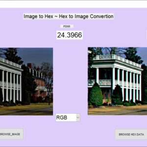
Efficient Image Conversion and Restoration System with Hexadecimal Encoding and Quality Evaluation
Abstract:
The proposed work aims to facilitate the conversion of images into a hexadecimal format for efficient storage and manipulation, and subsequently restore them to their original form. This conversion is beneficial for reducing storage space and simplifying data transmission. The system supports multiple color spaces, including grayscale, RGB, and YCbCr, enhancing its versatility in image processing tasks. Users select an image file, which the system processes according to the selected mode: converting the image or its channels to a hexadecimal format and saving the data to files. During restoration, the system reads the hexadecimal files, reconstructs the image, and displays it. To ensure the fidelity of the restored images, the system computes and displays quality metrics such as Peak Signal-to-Noise Ratio (PSNR), Mean Squared Error (MSE), and Structural Similarity Index (SSIM). This comprehensive solution provides an efficient method for image data handling and quality assessment, ensuring accurate and reliable image restoration.
Proposed System:The proposed system aims to facilitate the conversion of images into a hexadecimal format and subsequently restore them to their original form. This system supports multiple color spaces, including grayscale, RGB, and YCbCr, and evaluates the quality of the restored images using metrics such as Peak Signal-to-Noise Ratio (PSNR), Mean Squared Error (MSE), and Structural Similarity Index (SSIM).
List of the following materials will be included with the Downloaded Backup: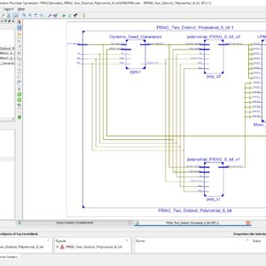
Efficient Pseudo Random Number Generator (PRNG) Design on FPGA
Proposed Abstract:
Random Number Generators (RNGs) are substantially used in many security domains, providing a fundamental source of unpredictability essential for tasks such as cryptography, simulations, and statistical analyses. The efficiency and quality of an RNG directly impact the reliability and security of diverse applications, making advancements in RNG design, as explored in this study, of significant importance for enhancing computational processes. This paper presents an innovative Pseudo-Random Number Generator (PRNG) that leverages the efficiency of two carefully selected Linear Feedback Shift Registers (LFSRs) and a connecting XOR gate. The investigation of five polynomials identified an optimal pair, resulting in a notable improvement of over 200X in the length of random bit sequences compared to a single LFSR-based PRNG. The Basys3 FPGA board with the xc7a35tcpg236-1 FPGA chip was used to implement and synthesize the proposed design. Two significant findings emerge from this research. Firstly, using variable polynomials demonstrates a huge enhancement in the duration of randomness, outperforming the impact of variable seeds. A noteworthy observation is that employing the same polynomials in different branches does not result in optimal results. Secondly, managing more seeds is associated with an increased area cost, underscoring the efficiency of handling two polynomials.
List of the following materials will be included with the Downloaded Backup:
Energy Efficient Compact Approximate Multiplier for Error-Resilient Applications
Base Paper Abstract:
The primary goal of approximate computing is enhancing system performance, such as energy efficiency, speed, and form factor. Despite the growing use of approximate multipliers, the design of efficient approximate compressors — a fundamental multiplier block — remains a significant challenge. In this brief, 8-transistor and 14-transistor 4:2 compressors are proposed. Both compressors exploit CMOS technology and a constant and conditional approximation of selected inputs, exhibiting fewer negative errors. As a result, a resource-expensive error recovery module is eliminated, yielding superior performance as compared with prior art. The 14-transistor architecture yields a lower error rate compared to the 8-transistor architecture, trading off lower area for higher accuracy. The compressor tailored circuit architecture is also proposed and evaluated using image multiplication. The proposed multiplier exhibits 50% area savings and 93% lower power-delay-product compared to the exact multiplier, as well as higher accuracy, and 38% PDP enhancement compared with the state-of-the-art.
List of the following materials will be included with the Downloaded Backup:
Energy-Efficient VLSI Realization of Binary64 Division With Redundant Number Systems
Base Paper Abstract:
VLSI realizations of digit-recurrence binary division usually use redundant representation of partial remainders and quotient digits. The former allows for fast carry-free computation of the next partial remainder, and the latter leads to less number of the required divisor multiples. In studying the previous relevant works, we have noted that the binary carry save (CS) number system is prevalent in the representation of partial remainders, and redundant high radix representation of quotient digits is popular in order to reduce the cycle count. In this paper, we explore a design space containing four division architectures. These are based on binary CS or radix-16 signed digit (SD) representations of partial remainders. On the other hand, they use full or partial pre computation of divisor multiples. The latter uses smaller multiplexer at the cost two extra adders, where one of the operands is constant within all cycles. The quotient digits are represented by radix-16 [−9,9]SDs. Our synthesis-based evaluation of VLSI realizations of the best previous relevant work and the four proposed designs show reduced power and energy figures in the proposed designs at the cost of more silicon area and delay measures. However, our energy-delay product is 26%–35% less than that of the reference work.
List of the following materials will be included with the Downloaded Backup:
ER-TCAM: A Soft-Error-Resilient SRAM-Based Ternary Content-Addressable Memory for FPGAs
Abstract:
Static random access memory (SRAM)-based ternary content-addressable memory (TCAM) on field-programmable gate arrays (FPGAs) is used for packet classification in software-defined networking (SDN) and Open Flow applications. SRAMs implementing TCAM contents constitute the major part of a TCAM design on FPGAs, which are vulnerable to soft errors. The protection of SRAM-based TCAMs against soft errors is challenging without compromising critical path delay and maintaining a high search performance. This brief presents a low cost and low-response-time technique for the protection of SRAM-based TCAMs. This technique uses simple, single-bit parity for fault detection which has a minimal critical path overhead. This technique exploits the binary-encoded TCAM table maintained in SRAM-based TCAMs for update purposes to implement a low-response-time error-correction mechanism at low cost. The error-correction process is carried out in the background, allowing lookup operations to be performed simultaneously, thus maintaining a high search performance. The proposed technique provides protection against soft errors with a response time of 293 ns, whereas maintaining a search rate of 222 million searches per second on a 1024 × 40 size TCAM on Artix-7 FPGA.
List of the following materials will be included with the Downloaded Backup:
Error Detection and Correction in SRAM Emulated TCAMs
Abstract:
Ternary content addressable memories (TCAMs) are widely used in network devices to implement packet classification. They are used, for example, for packet forwarding, for security, and to implement software-defined networks (SDNs). TCAMs are commonly implemented as standalone devices or as an intellectual property block that is integrated on networking application-specific integrated circuits. On the other hand, field-programmable gate arrays (FPGAs) do not include TCAM blocks. However, the flexibility of FPGAs makes them attractive for SDN implementations, and most FPGA vendors provide development kits for SDN. Those need to support TCAM functionality and, therefore, there is a need to emulate TCAMs using the logic blocks available in the FPGA. In recent years, a number of schemes to emulate TCAMs on FPGAs have been proposed. Some of them take advantage of the large number of memory blocks available inside modern FPGAs to use them to implement TCAMs. A problem when using memories is that they can be affected by soft errors that corrupt the stored bits. The memories can be protected with a parity check to detect errors or with an error correction code to correct them, but this requires additional memory bits per word. In this brief, the protection of the memories used to emulate TCAMs is considered. In particular, it is shown that by exploiting the fact that only a subset of the possible memory contents are valid, most single-bit errors can be corrected when the memories are protected with a parity bit.
List of the following materials will be included with the Downloaded Backup:
Feed forward-Cutset-Free Pipelined Multiply–Accumulate Unit for the Machine Learning Accelerator
Abstract:
Multiply–accumulate (MAC) computations account for a large part of machine learning accelerator operations. The pipelined structure is usually adopted to improve the performance by reducing the length of critical paths. An increase in the number of flip-flops due to pipelining, however, generally results in significant area and power increase. A large number of flip-flops are often required to meet the feed forward-cutset rule. Based on the observation that this rule can be relaxed in machine learning applications, we propose a pipelining method that eliminates some of the flip-flops selectively. The simulation results show that the proposed MAC unit achieved a 20% energy saving and a 20% area reduction compared with the conventional pipelined MAC.
List of the following materials will be included with the Downloaded Backup: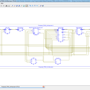
FPGA Based True Random Number Generation Using Programmable Delays in Oscillator Rings
Abstract:
True random number generators play a fundamental role in cryptographic systems. This paper presents a new and efficient method to generate true random numbers on field programmable gate array by utilizing the random jitter of free running oscillators as a source of randomness. The free-running oscillator rings incorporate programmable delay lines to generate large variation of the oscillations and to introduce jitter in the generated ring oscillators clocks. The main advantage of the proposed true random number generator utilizing programmable delay lines is to reduce correlation between several equal length oscillator rings, and thus improve the randomness qualities. In addition, a Von Neumann corrector as post-processor is employed to remove any bias in the output bit sequence. The validation of the proposed approach is demonstrated on Xilinx Spartan-3A FPGAs. The proposed true random number generator occupies 528 slices, achieves 6 Mbps throughput with 0.999 per bit entropy rate, and passes all the National Institute of Standards and Technology (NIST) statistical tests.
List of the following materials will be included with the Downloaded Backup: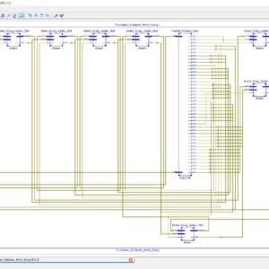
FPGA Implementation of 8×8 Truncated Multiplier Using Brent Kung Parallel Prefix Adder
Proposed Abstract:
Multiplication is a critical operation in many digital signal processing and machine learning applications, where fast and efficient computation is essential. However, conventional multipliers that compute n x n bit products result in significant hardware overhead and increased power consumption. To address these challenges, this paper proposes an FPGA implementation of an 8x8 truncated multiplier utilizing the Brent-Kung parallel prefix adder to improve both speed and resource efficiency. The proposed truncated multiplier limits the output to n bits, discarding the least significant bits and utilizing a variable correction technique to minimize the error introduced by truncation. By selectively summing the most significant columns, the design achieves a balance between accuracy and hardware efficiency, providing a reduced-area solution for approximate computing. The Brent-Kung parallel prefix adder is integrated into the multiplier architecture to optimize the carry propagation stage, reducing the overall critical path delay. This adder is known for its logarithmic depth, which significantly improves the speed of the summation process while using fewer logic gates compared to traditional adders. This design was implemented in Verilog HDL and synthesized on a Xilinx Virtex-5 FPGA platform. Comparative analysis with a conventional multiplier shows that the proposed truncated multiplier achieves a notable reduction in FPGA resource utilization, including logic elements and power consumption, without sacrificing significant accuracy. The architecture particularly suitable for applications where speed and low power consumption are paramount, such as real-time image processing, DSP systems, and machine learning accelerators.
List of the following materials will be included with the Downloaded Backup: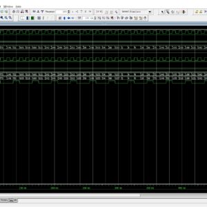
FPGA Implementation of Comparative Analysis and Performance Evaluation for Different LFSR Techniques
Proposed Abstract:
In this study, we explore the implementation and performance evaluation of various Linear Feedback Shift Register (LFSR) techniques on Field Programmable Gate Arrays (FPGAs). LFSRs are fundamental components in numerous digital applications, including cryptography, pseudorandom number generation, error detection, and secure communications. We specifically focus on five different LFSR methodologies: Fibonacci LFSR, Galois LFSR, Non-Linear Feedback Shift Register (NLFSR), Modular LFSR and Masked LFSR. Each technique is implemented on an FPGA platform, utilizing Verilog HDL for design specification and synthesis. The study begins with a detailed examination of the theoretical underpinnings and operational mechanisms of each LFSR technique, followed by their FPGA implementations. We then conduct a comprehensive performance analysis, focusing on critical parameters such as area utilization, power consumption, throughput, and randomness quality. The analysis reveals the strengths and trade-offs associated with each method, providing insights into their suitability for various applications. Our results demonstrate that while Fibonacci and Galois LFSRs offer simplicity and ease of implementation, more advanced techniques like NLFSR and Masked LFSR provide enhanced security features at the cost of increased complexity. The study concludes with recommendations on selecting the appropriate LFSR technique based on the specific requirements of the application, highlighting the balance between security, performance, and resource efficiency in FPGA-based designs.
List of the following materials will be included with the Downloaded Backup: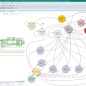
FPGA Implementation of Intelligent Elevator System for AI Applications
Proposed Abstract:
Intelligent elevator systems are used in many smart buildings, offices, hospitals, and tall apartments to move people quickly, reduce waiting time, and save energy. They have many advantages, like faster operation, better safety, and the ability to handle requests from many floors at the same time. But there are also some disadvantages, such as slow response when many people use them, fixed movement patterns that cannot adjust to real-time needs, weak security for restricted floors, and no use of advanced AI features for learning and prediction. Most existing elevator systems are built using microcontrollers with fixed scheduling methods, which cannot easily change their operation or add smart features. The problem in this work is to create an elevator system that works faster, is more secure, can adjust to different situations, and is ready for AI use, while also keeping passengers safe. In this project, we design an elevator controller on FPGA using a finite state machine. The system includes floor request handling, priority scheduling, emergency stop, overload detection, automatic door timing, floor number display, passcode access for special floors, and a fire alarm mode. The new idea in this work is to use the speed and flexibility of FPGA hardware along with an FSM design that can later connect to AI for learning passenger habits and predicting movement needs. This makes the system quick, safe, and adaptable. The design is written in Verilog HDL, tested in ModelSim, and implemented on a Xilinx FPGA board. We measure performance by checking response time, scheduling efficiency, and safety accuracy, and the results show it is suitable for future smart building use.
List of the following materials will be included with the Downloaded Backup: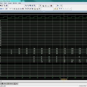
FPGA Implementation of Partially Parallel Encoder Architecture for Long Polar Code
Polar coding is an encoding/decoding scheme that provably achieves the capacity of the class of symmetric binary memory-less channels. Due to the channel achieving property, the polar code has become one of the most favourable error-correcting codes. As the polar code achieves the property asymptotically, however, it should be long enough to have a good error-correcting performance. Although previous fully parallel encoder is intuitive and easy to implement, it is not suitable for long polar codes because of the huge hardware complexity required. In the brief, we analyse the encoding process in the viewpoint of very large-scale integration implementation and propose a new efficient encoder architecture that is adequate for long polar codes and effect in alleviating the hardware complexity. As the proposed encoder allows high-throughput encoding with small hardware complexity, it can be systematically applied to the design of any polar code and to any level of parallelism. Finally shown the power, area, delay report with comparison of existing work.
List of the following materials will be included with the Downloaded Backup:
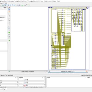
FPGA Implementation of Single Precision Floating Point Multiplier using High Speed Parallel Prefix Adder based Wallace Tree Multiplier
Base Paper Abstract:
In this paper present, an efficient implementation of single precision method of floating point multiplier target for Xilinx Vertex 5 FPGA using Verilog HDL. The floating point implementation will cover up with 23-bit exponent, 8-bit mantissa, and 1 sign bit. This proposed architecture implement with high speed parallel prefix adder based Wallace Tree Multiplier. a Wallace tree multiplication will provide effective terms of low logic sizes and more speed of operations. In a recent arithmetic applications based circuit design will have more demand with high speed and low area, in this manner the proposed approach of this work will improve the speed of Wallace tree multiplier using 4:2 compressor method without degrading its area parameter. Thus, the proposed method will integrate more efficient and more reliable Kogge stone parallel prefix, Brent kung parallel prefix, Sklansky parallel prefix addition operation in the Wallace tree multiplication on final addition stage at 16-bit data width. Finally, done this floating point multiplier architecture with Wallace tree architecture included normalized rounding method and to reduce area, delay and power. The error difference will have analyzed using Modelsim Software, and analyses optimized logic size's, delay and power consumptions.
List of the following materials will be included with the Downloaded Backup: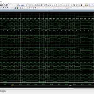
Fully Reused VLSI Architecture of FM0Manchester Encoding Using SOLS Technique for DSRC Applications
The dedicated short-range communication (DSRC) is an emerging technique to push the intelligent transportation system into our daily life. The DSRC standards generally adopt FM0 and Manchester codes to reach dc-balance, enhancing the signal reliability. Nevertheless, the coding-diversity between the FM0 and Manchester codes seriously limits the potential to design a fully reused VLSI architecture for both. In this paper, the similarity-oriented logic simplification (SOLS) technique is proposed to overcome this limitation. The encoding capability of this paper can fully support the DSRC standards of America, Europe, and Japan. This paper not only develops a fully reused VLSI architecture, but also exhibits an efficient performance compared with the existing works. The proposed architecture of this paper analysis the logic size, area and power consumption using Xilinx 14.2.
List of the following materials will be included with the Downloaded Backup:
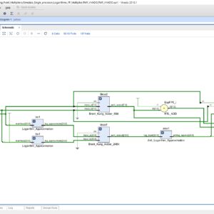
Hardware-Efficient Logarithmic Floating-Point Multipliers for Error-Tolerant Applications
Base Paper Abstract:
The increasing computational intensity of important new applications poses a challenge for their use in resource restricted devices. Approximate computing using power-efficient arithmetic circuits is one of the emerging strategies to reach this objective. In this article, five hardware-efficient logarithmic floating-point (FP) multipliers are proposed, which all use simple operators, such as adders and multiplexers, to replace complex and costlier conventional FP multipliers. Radix-4 logarithms are used to further reduce the hardware complexity. These designs produce double-sided error distributions to mitigate error accumulation in complex computations. The proposed multipliers provide superior trade-offs between accuracy and hardware, with up to 30.8% higher accuracy than a recent logarithmic FP design or up to 68× less energy than the conventional FP multiplier. Using the proposed FP logarithmic multipliers in JPEG image compression achieves higher image quality than a recent logarithmic multiplier design with up to 4.7 dB larger peak signal-to-noise ratio. For training in benchmark NN applications, the proposed FP multipliers can slightly improve the classification accuracy while achieving 4.2× less energy and 2.2× smaller area than the state-of-the-art design.
List of the following materials will be included with the Downloaded Backup: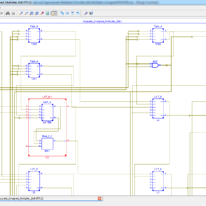
High Performance Accurate and Approximate Multipliers for FPGA based Hardware Accelerators
Abstract:
Multiplication is one of the widely used arithmetic operations in a variety of applications, such as image/video processing and machine learning. FPGA vendors provide high performance multipliers in the form of DSP blocks. These multipliers are not only limited in number and have fixed locations on FPGAs but can also create additional routing delays and may prove inefficient for smaller bit-width multiplications. Therefore, FPGA vendors additionally provide optimized soft IP cores for multiplication. However, in this work, we advocate that these soft multiplier IP cores for FPGAs still need better designs to provide high-performance and resource efficiency. Towards this, we present generic area-optimized, low-latency accurate and approximate soft-core multiplier architectures, which exploit the underlying architectural features of FPGAs, i.e., look-up table (LUT) structures and fast carry chains to reduce the overall critical path delay and resource utilization of multipliers. Compared to Xilinx multiplier LogiCORE IP, our proposed unsigned and signed accurate architecture provides up to 25% and 53% reduction in LUT utilization, respectively, for different sizes of multipliers. Moreover, with our unsigned approximate multiplier architectures, a reduction of up to 51% in the critical path delay can be achieved with an insignificant loss in output accuracy when compared with the LogiCORE IP. For illustration, we have deployed the proposed multiplier architecture in accelerators used in image and video applications, and evaluated them for area and performance gains.
List of the following materials will be included with the Downloaded Backup: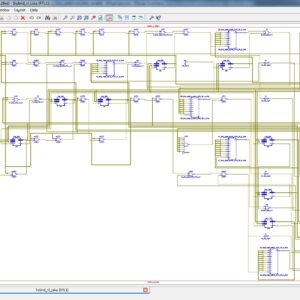
High Speed and Energy Efficient Carry Skip Adder Operating Under a Wide Range of Supply Voltage Levels
Abstract:
In this paper, we present a carry skip adder (CSKA) structure that has a higher speed yet lower energy consumption compared with the conventional one. The speed enhancement is achieved by applying concatenation and incrimination schemes to improve the efficiency of the conventional CSKA (Conv-CSKA) structure. In addition, instead of utilizing multiplexer logic, the proposed structure makes use of NAND-NOR-Invert (NNI) and NOR-NAND-Invert (NNI) compound gates for the skip logic. The structure may be realized with both fixed stage size and variable stage size styles, wherein the latter further improves the speed and energy parameters of the adder. Finally, a hybrid variable latency extension of the proposed structure, which lowers the power consumption without considerably impacting the speed, is presented. This extension utilizes a modified parallel structure for increasing the slack time, and hence, enabling further voltage reduction. The proposed architecture of this paper analysis the logic size, area and power consumption using Xilinx 14.2.
List of the following materials will be included with the Downloaded Backup: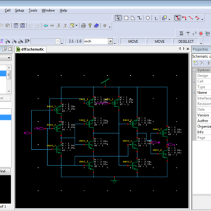
High speed and low power preset-able modified TSPC D flip-flop design and performance comparison with TSPC D flip-flop
Abstract:
Positron emission tomography (PET) is a nuclear functional imaging technique that produces a three-dimensional image of functional organs in the body. PET requires high resolution, fast and low power multichannel analog to digital converter (ADC). A typical multichannel ADC for PET scanner architecture consists of several blocks. Most of the blocks can be designed by using fast, low power D flip-flops. A preset-able true single phase clocked (TSPC) D flip-flop shows numerous glitches (noise) at the output due to unnecessary toggling at the intermediate nodes. Preset-able modified TSPC (MTSPC) D flip flop have been proposed as an alternative solution to alleviate this problem. However, the MTSPC D flip-flop requires one extra PMOS to suspend toggling of the intermediate nodes. In this work, we designed a 7-bit preset-able gray code counter by using the proposed D flip-flop. This work involves UMC 180 nm CMOS technology for preset-able 7-bit gray code counter where we achieved 1 GHz maximum operation frequency with most significant bit (MSB) delay 0.96 ns, power consumption 244.2 μW (micro watt) and power delay product (PDP) 0.23 pJ (Pico joule) from 1.8 V power supply.
List of the following materials will be included with the Downloaded Backup: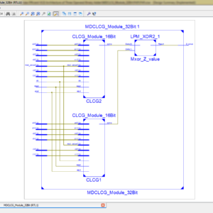
High Speed Area Efficient VLSI Architecture of Three Operand Binary Adder
Abstract:
Three-operand binary adder is the basic functional unit to perform the modular arithmetic in various cryptography and pseudorandom bit generator (PRBG) algorithms. Carry save adder (CS3A) is the widely used technique to perform the three-operand addition. However, the ripple-carry stage in the CS3A leads to a high propagation delay of O(n). Moreover, a parallel prefix two-operand adder such as Han-Carlson (HCA) can also be used for three-operand addition that significantly reduces the critical path delay at the cost of additional hardware. Hence, a new high-speed and area-efficient adder architecture is proposed using pre-compute bitwise addition followed by carry prefix computation logic to perform the three-operand binary addition that consumes substantially less area, low power and drastically reduces the adder delay to O(log2 n). The proposed architecture is implemented on the FPGA device for functional validation and also synthesized with the commercially available 32nm CMOS technology library. The post-synthesis results of the proposed adder reported 3.12, 5.31 and 9.28 times faster than the CS3A for 32-, 64- and 128- bit architecture respectively. Moreover, it has a lesser area, lower power dissipation and smaller delay than the HC3A adder. Also, the proposed adder achieves the lowest ADP and PDP than the existing three-operand adder techniques.
List of the following materials will be included with the Downloaded Backup: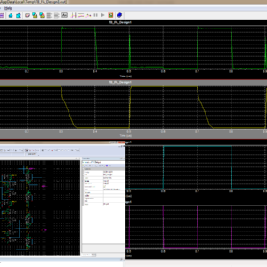
High-Speed Hybrid-Logic Full Adder Using High-Performance 10-T XOR–XNOR Cell
Abstract:
Hybrid logic style is widely used to implement full adder (FA) circuits. Performance of hybrid FA in terms of delay, power, and driving capability is largely dependent on the performance of XOR–XNOR circuit. In this article, a high speed, low-power 10-T XOR–XNOR circuit is proposed, which provides full swing outputs simultaneously with improved delay performance. The performance of the proposed circuit is measured by simulating it in cadence virtuoso environment using 90-nm CMOS technology. The proposed circuit reduces the power delay product (PDP) at least by 7.5% than that of the available XOR–XNOR modules. Four different designs of FAs are also proposed in this article utilizing the proposed XOR–XNOR circuit and available sum and carry modules. The proposed FAs provide 2%–28.13% improvement in terms of PDP than that of other architectures. To measure the driving capabilities, the proposed FAs are embedded in 2-, 4-, and 8-bit cascaded full adder (CFA) structures. Results show that two of the proposed FAs provide the best performance for a higher number of bits among all the FAs.
List of the following materials will be included with the Downloaded Backup: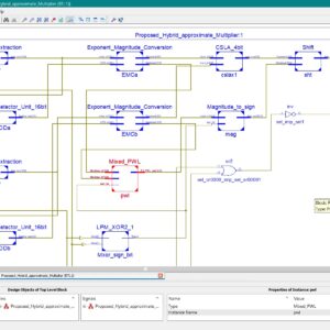
Hybrid Approximate Multipliers with Merits Balance for Digital Processing and Neural Networks
In this article, hybrid approximate multiplier (HAMs) designs based on the combination of logarithmic multiplication and piecewise linear (PWL) fitting are proposed. After extracting the exponent and mantissa of the input operands, two new variables are introduced to perform spatial mixed linear fitting on the 3-D surface of the mantissa product in different regions. Limited power-of-2 elements in line slopes make the multivariable mixed PWL computational simple and friendly to logic circuit complexity. With iterative adjustment of the slopes and bias of the lines in the PWL calculation, the relative error distance (RED) distribution is well balanced and zero concentrated. In addition, we detail the logic architecture to implement approximate hybrid accumulation and error tolerant complement conversions. In the 45-nm library-based performance comparison, the proposed multipliers mainly 16-, 8-, and 32-bit floating-point multipliers exhibit >55% power, >23% delay, and >43% area reductions compared with the exact multiplier. In addition, they outperform other state-of-the-art designs in terms of delay, power, area, and error, as evaluated by the joint delay–power–area product (PPA) and mean RED (MRED). In case experiments, the proposed multipliers perform nearly equivalently to the exact multiplier in error-tolerant digital processing and neural network computations. Index Terms Approximate multiplier, arithmetic digital circuit, computational logic architecture, logarithmic multiplier, piecewise linear (PWL).
List of the following materials will be included with the Downloaded Backup: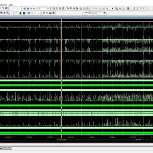
Implementation of High-Precision MFCC Feature Extraction Using FPGA for Speech Recognition
Proposed Abstract:
Speaker recognition is one of the technologies that may be used for biometric identification, and it offers higher application possibilities in many sectors. At the moment, the implementation of the speaker identification algorithm on the hardware is mostly dependent on the SOC of the FPGA. An FPGA-based real-time technique for extracting acoustic characteristics is presented in this research. The method is based on MFCC, which stands for Mel Frequency Cepstral Coefficients. The trials have shown that the FPGA-based MFCC calculation has a high level of accuracy; the purpose of this study is to enhance the performance assessment of MFCC by making use of novelty-based architecture. In this study, a technique for FPGA-based speech recognition is provided. This approach was developed by investigation and analysis of the speaker recognition algorithm. The IFFT, the Mell filter, the DFT, the derivatives, and the Hamming Window with pre-emphasis are every aspect of this approach. This proposed MFCC will be constructed with an AHB interface in order to facilitate higher access DMA Controller when it is used in SOC applications. This work was carried out using Verilog HDL, and it was generated with Xilinx Vivado FPGA. Additionally, all of the parameters were analyzed and compared with regard to area, latency, and power.
List of the following materials will be included with the Downloaded Backup: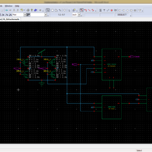
Implementation of Low Power 1-bit Hybrid Full Adder using 22nm CMOS Technology
Abstract:
Adders are plays a vital role in digital and vlsi systems. Arithmetic operations are an essential part of digital systems. During VLSI systems, the entire research is on lowering the scale of transistors for enforcing any other digital system. This proposed architecture implemented by different types of logic systems; each logic performs the different role in the hybrid system. The hybrid Full Adder cell with one bit is implemented in this structure. The proposed method is investigated using 22-nm CMOS hybrid full adder. The proposed architecture demonstrates substantial efficiency in power consumption and delay, based on simulation results. The simulation result expressed that the full adder circuit is used to modern high speed central processing unit in the data path architecture. This form of hybrid Full Adder, reduces the delay and increasing efficiency and mainly used in nano technology applications. The average power consumption of 1.1055uW with moderately low delay of 7.0415 ps was found to be extremely low for 0.8-V supply at 22-nm technology. These kind of adder allocates significant improvements in power, high speed and area compared with previous full adder designs.
List of the following materials will be included with the Downloaded Backup: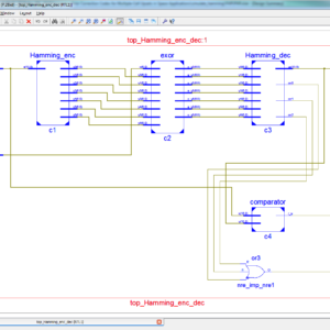
Improving Error Correction Codes for Multiple-Cell Upsets in Space Applications
Proposed Abstract:
Currently, faults suffered by SRAM memory systems have increased due to the aggressive CMOS integration density. Thus, the probability of occurrence of single-cell upsets (SCUs) or multiple-cell upsets (MCUs) augments. One of the main causes of MCUs in space applications is cosmic radiation. A common solution is the use of error correction codes (ECCs). Nevertheless, when using ECCs in space applications, they must achieve a good balance between error coverage and redundancy, and their encoding/decoding circuits must be efficient in terms of area, power, and delay. Different codes have been proposed to tolerate MCUs. For instance, Matrix codes use Hamming codes and parity checks in a bi-dimensional layout to correct and detect some patterns of MCUs. Recently presented, column–line–code (CLC) has been designed to tolerate MCUs in space applications. CLC is a modified Matrix code, based on extended Hamming codes and parity checks. Nevertheless, a common property of these codes is the high redundancy introduced. In this paper, we present a series of new low redundant ECCs able to correct MCUs with reduced area, power, and delay overheads. Also, these new codes maintain, or even improve, memory error coverage with respect to Matrix and CLC codes.
List of the following materials will be included with the Downloaded Backup: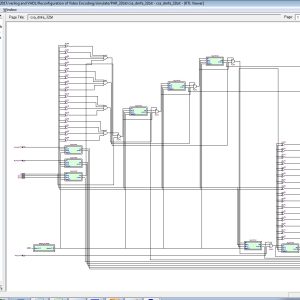
Input Based Dynamic Reconfiguration of Approximate Arithmetic Units for Video Encoding
Abstract:
The field of approximate computing has receivedsignificant attention from the research community in the pastfew years, especially in the context of various signal processingapplications. Image and video compression algorithms, such asJPEG, MPEG, and so on, are particularly attractive candidatesfor approximate computing, since they are tolerant of computingimprecision due to human imperceptibility, which can beexploited to realize highly power-efficient implementations ofthese algorithms. However, existing approximate architecturestypically fix the level of hardware approximation staticallyand are not adaptive to input data. For example, if afixed approximate hardware configuration is used for anMPEG encoder (i.e., a fixed level of approximation), theoutput quality varies greatly for different input videos. Thispaper addresses this issue by proposing a reconfigurableapproximate architecture for MPEG encoders thatoptimizespower consumption with the goal of maintaining a particularPeak Signal-to-Noise Ratio (PSNR) threshold for any video.We propose two heuristics for automaticallytuning the approximation degree of the RABs in thesetwo modules during runtime based on the characteristics of eachindividual video. The proposed architecture of this paper analysis the logic size, area and power consumption using Xilinx 14.2.
List of the following materials will be included with the Downloaded Backup: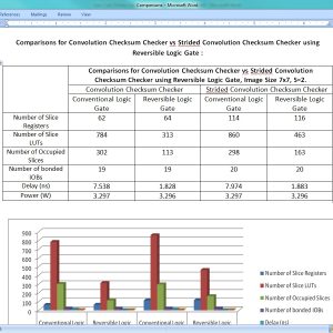
Low Cost Online Convolution Checksum Checker
Abstract:
Managing random hardware faults requires the faults to be detected online, thus simplifying recovery. Algorithm-based fault tolerance has been proposed as a low-cost mechanism to check online the result of computations against random hardware failures. In this case, the checksum of the actual result is checked against a predicted checksum computed in parallel by a hardware checker. In this work, we target the design of such checkers for convolution engines that are currently the most critical building block in image processing and computer vision applications. The proposed convolution checksum checker, named ConvGuard, utilizes a newly introduced invariance condition of convolution to predict implicitly the output checksum using only the pixels at the border of the input image. In this way, ConvGuard reduces the power required for accumulating the input pixels without requiring large buffers to hold intermediate checksum results. The design of ConvGuard is generic and can be configured for different output sizes and strides. The experimental results show that ConvGuard utilizes only a small percentage of the area/power of an efficient convolution engine while being significantly smaller and more power efficient than a state-of-the-art checksum checker for various practical cases.
List of the following materials will be included with the Downloaded Backup: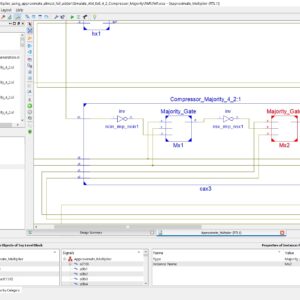
Low power Dadda multiplier using approximate almost full adder and Majority logic based adder compressors
Base Paper Abstract:
An Approximate computing is widely used to have energy-efficient system design in Very Large-Scale Integration (VLSI). This approach is best suited for signal processing and multimedia applications where low power consumption is the main concern. Faster and significant results can be obtained from an approximate computing at the cost of reduced accuracy. In this work, we proposed a very novel design approaches based on various monolithic 4:2 compressors. Proposed approach is applied to have reduced stages in the partial product multiplication. Proposed Monolithic compressor had outperformed over various 4:2 compressors. Our proposed method is based on majority logic based with the use of Dadda multiplication. A new-partial product reduction format is implemented by this multiplier, which reduces the maximum output delay. This method of approach significantly reduces the utilization of number of MOSFETs compared to other multiplier such as Wallace Tree Multipliers. Simulation results are compared with conventional Dadda multiplier and ML based 4:2 compressors. Proposed approximate computing based almost full adder based majority logic based Dadda multiplier achieves reduction of 60.93% in area utilization 72.48% reduction in dynamic power reduction while processing time is also reduced by 72.98%. Dadda multiplication outperforms the other compressors.
List of the following materials will be included with the Downloaded Backup:
Low Power Divider Using Vedic Mathematics
Vedic mathematics is a unique technique of carrying out mathematical computations and it has its roots in the ancient Indian Mathematics. This paper presents the divider architecture using one of the Vedic mathematics techniques called as Paravartya-Yojayet, which means to transpose and apply. This paper proposes a fast, low power and cost effective architecture of a divider using the ancient Indian Vedic division algorithm. The merits of the proposed architecture are proved by comparing the gate count, power consumption and delay against the conventional divider architectures. The proposed architecture of this paper analysis the logic size, area and power consumption using Xilinx 14.2.
List of the following materials will be included with the Downloaded Backup:
Low Power Variation Tolerant Nonvolatile Lookup Table Design
Emerging nonvolatile memories (NVMs), such as MRAM, PRAM, and RRAM, have been widely investigated to replace SRAM as the configuration bits in field-programmable gate arrays (FPGAs) for high security and instant power ON. However, the variations inherent in NVMs and advanced logic process bring reliability issue to FPGAs. This brief introduces a low-power variation-tolerant nonvolatile lookup table (nvLUT) circuit to overcome the reliability issue. Because of large ROFF/RON, 1T1R RRAM cell provides sufficient sense margin as a configuration bit and a reference resistor. A single-stage sense amplifier with voltage clamp is employed to reduce the power and area without impairing the reliability. Matched reference path is proposed to reduce the parasitic RC mismatch for reliable sensing. Evaluation shows that 22% reduction in delay, 38% reduction in power, and the tolerance of variations of 2.5× typical RON or ROFF in reliability are achieved for proposed nvLUT with six inputs. The proposed architecture of this paper area and power consumption analysis using tanner tool.
List of the following materials will be included with the Downloaded Backup:
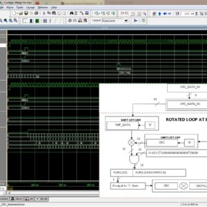
Low-Cost and Programmable CRC Implementation Based on FPGA
Abstract:
Cyclic redundancy check (CRC) is a well-known error detection code that is widely used in Ethernet, PCIe, and other transmission protocols. The existing FPGA-based implementation solutions encounter the problem of excessive resource utilization in high-performance scenarios. The padding zeros problem and the introduction of programmability further exacerbate this problem. In this brief, the stride-by-5 algorithm is proposed to achieve the optimal utilization of FPGA resources. The pipelining go back algorithm is proposed to solve the padding zeros problem. The method of reprogramming by HWICAP is proposed to realize programmability with small and constant resource utilization. The experimental results show that the resource utilization of the proposed non-segmented architecture is 80.7%-87.5% and 25.1%-46.2% lower than that of two state of-the-art FPGA-based CRC implementations, and the proposed segmented architecture has lower resource utilization, by 81.7%- 85.9% and 2.9%-20.8%, than two state-of-the-art architectures. Furthermore, throughput and programmability are guaranteed.
List of the following materials will be included with the Downloaded Backup: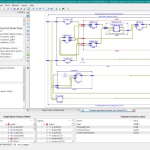
Low-Power High Precision Floating-Point Divider with Bidimensional Linear Approximation
Base Paper Abstract:
In this paper we propose a novel approximate floating-point divider based on bi-dimensional linear approximation. In our approach, the mantissa quotient is seen as a function of the two input mantissas of the divider. The domain of this two-variable function is partitioned into nx × ny subregions, named tiles, where nx, ny are chosen as powers of two. In each tile the quotient is approximated with a linear combination of the input mantissas. To achieve fine accuracy, an optimization problem is formulated within each tile to determine the optimal coefficients for the linear combination, which minimize the Mean Relative Error Distance (MRED) of the divider. Furthermore, to make hardware implementation more effective, the minimization problem is appropriately modified to search for optimal quantized coefficients. The hardware structure of the divider only requires a small look-up table to store the linear approximation coefficients, and a carry save adder tree. The proposed architecture is highly tunable at design-time over a wide range of accuracy, depending on the number of tiles chosen for the approximation. The obtained results demonstrate error performance and hardware features superior to the state-of-the-art. The proposed dividers define the Pareto front, considering the trade-off between power-delay-product vs. MRED and area-delay-product vs. MRED, for MRED in the range of 4 × 10⁻³ − 2 × 10⁻². Application results for JPEG compression and tone mapping further highlight the strength of our proposal, which exhibits Structural Similarity Index (SSIM) very close to 1 in all cases and Peak Signal-to-Noise Ratio (PSNR) up to 45 db. Index Terms: Floating-point divider, approximate computing, error correction, low-power.
List of the following materials will be included with the Downloaded Backup: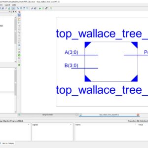
Modified Wallace Tree Multiplier using Efficient Square Root Carry Select Adder
A multiplier is one of the key hardware blocks in most digital and high performance systems such as FIR filters, micro processors and digital signal processors etc. A system’s performance is generally determined by the performance of the multiplier because the multiplier is generally the slowest element in the whole system and also it is occupying more area consuming. The Carry Select Adder (CSLA) provides a good compromise between cost and performance in carry propagation adder design. A Square Root Carry Select Adder using RCA is introduced but it offers some speed penalty. However, conventional CSLA is still area-consuming due to the dual ripple carry adder structure. In the proposed work, generally in Wallace multiplier the partial products are reduced as soon as possible and the final carry propagation path carry select adder is used. In this paper, modification is done at gate level to reduce area and power consumption. The Modified Square Root Carry Select-Adder (MCSLA) is designed using Common Boolean Logic and then compared with regular CSLA respective architectures, and this MCSLA is implemented in Wallace Tree Multiplier. This work gives the reduced area compared to normal Wallace tree multiplier. Finally an area efficient Wallace tree multiplier is designed using common Boolean logic based square root carry select adder.
List of the following materials will be included with the Downloaded Backup:
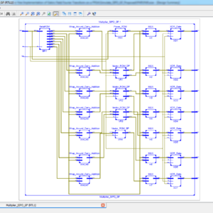
Multiplier-free Implementation of Galois Field Fourier Transform on a FPGA
Abstract:
A novel approach to implementing Galois Field Fourier Transform (GFT) is proposed that completely eliminates the need for any finite field multipliers by transforming the symbols from a vector representation to a power representation. The proposed method is suitable for implementing GFTs of prime and nonprime lengths on modern FPGAs that have a large amount of on-chip distributed embedded memory. For GFT of length 255 that is widely used in many applications, the proposed memory based implementation exhibits 25% improvement in latency, 27% improvement in throughput, and 56% reduction in power consumption compared to a finite field multiplier based implementation.
List of the following materials will be included with the Downloaded Backup: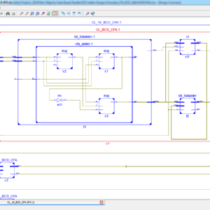
New Majority Gate Based Parallel BCD Adder Designs for Quantum-dot Cellular Automata
Abstract:
In this paper, we first theoretically re-defined output decimal carry in terms of majority gates and proposed a carry look ahead structure for calculating all the intermediate output carries. We have used this method for designing the multi-digit decimal adders. Theoretically, our best n-digit decimal adder design reduces the delay and area-delay product (ADP) by 50% compared with previous designs. We have implemented our designs using QCA Designer tool. The proposed QCA Designer based 8-digit PBA-BCD adder achieves over 38% less delay compared with the best existing designs.
List of the following materials will be included with the Downloaded Backup: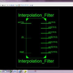
Novel Block-Formulation and Area-Delay-Efficient Reconfigurable Interpolation Filter Architecture for Multi-Standard SDR Applications
Abstract: The input-matrix and the coefficient-matrix resizes when changes. An analysis of interpolation filter computation for different up-sampling factors is made in this paper to identify redundant computations and removed those by reusing partial results. Reuse of partial results eliminates the necessity of matrix resizing in interpolation filter computation. A novel block-formulation is presented to share the partial results for parallel computation of filter outputs of different up-sampling factors. Using the proposed block formulation, to increase the number of tab to 16 and to get the accuracy and reduce the delay. The proposed architecture of this paper analysis the logic size, area and power consumption using Xilinx 14.2.
List of the following materials will be included with the Downloaded Backup:
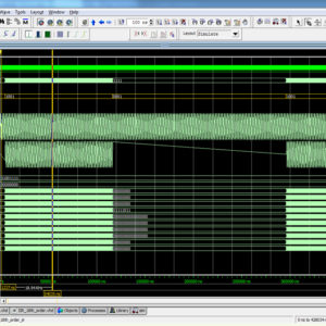
Obfuscating DSP Circuits via High Level Transformations
This paper presents a novel approach to design obfuscated circuits for digital signal processing (DSP) applications using high-level transformations, a key-based obfuscating finite-state machine (FSM), and a reconfigurator. The goal is to design DSP circuits that are harder to reverse engineer. High level transformations of iterative data-flow graphs have been exploited for area-speed-power tradeoffs. This is the first attempt to develop a design flow to apply high level transformations that not only meet these tradeoffs but also simultaneously obfuscate the architectures both structurally and functionally. Functional obfuscation is accomplished by requiring use of the correct initialization key, and configure data. Structural obfuscation is also achieved by the proposed methodology via high-level transformations. The proposed architecture of this paper analysis the logic size, area and power consumption using Xilinx 14.2
List of the following materials will be included with the Downloaded Backup:
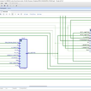
Optimized Dual Accumulator based RISC Architecture with Advanced Memory and Peripheral Operations
Proposed Abstract:
This paper presents an optimized Reduced Instruction Set Computer (RISC) architecture that leverages a dual accumulator design to enhance computational efficiency and performance. The architecture is scheduled to support advanced memory management and peripheral operations, addressing the growing need for high-speed data processing in embedded systems. The dual accumulator approach allows for parallel execution of arithmetic operations, reducing the number of instruction cycles and improving overall throughput. The architecture is designed with a focus on optimizing area, delay, and power consumption, making it suitable for resource-constrained environments. The proposed design is implemented using Verilog HDL and synthesized on the Xilinx Vivado platform targeting the Zynq FPGA. The architecture’s performance is verified through extensive simulation in Modelsim, and a comparative analysis is conducted to evaluate the improvements in key parameters such as area utilization, processing delay, and power efficiency. The results demonstrate that the optimized dual accumulator-based RISC architecture significantly outperforms traditional single accumulator designs, making it an ideal solution for modern embedded applications that require both high performance and low power consumption.
List of the following materials will be included with the Downloaded Backup: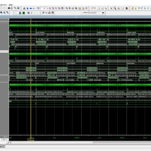
Optimizing Ternary Multiplier Design with Fast Ternary Adder
Base Paper Abstract:
Existing ternary multiplier designs are difficult to use in ternary systems. Thus, ternary Wallace tree multipliers that reduce the number of transistors by using 4-input ternary adders are proposed to improve the performance of existing ternary multipliers. A ternary carry-select adder is also proposed to reduce the carry propagation delay, used as a carry-chain adder of the Wallace tree. The proposed multipliers are designed with a custom ternary standard cell library synthesized by multi-threshold complementary metal-oxide-semiconductor (CMOS) with a 28 nm process. Power and delay are verified via HSPICE simulation. The proposed 36 × 36 ternary multiplier shows 79.3% power-delay product improvement over the previous ternary multiplier. The proposed 40 × 40 ternary multiplier shows a power-delay product comparable with that of the 64 × 64 binary multiplier synthesized using Synopsys Design Compiler.
List of the following materials will be included with the Downloaded Backup: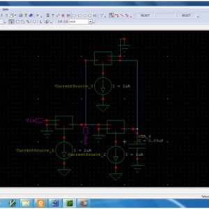
OTA-Based Logarithmic Circuit for Arbitrary Input Signal and Its Application
In this paper, a new design procedure has been proposed for realization of logarithmic function via three phases: 1) differentiation; 2) division; and 3) integration for any arbitrary analog signal. All the basic building blocks, i.e., differentiator, divider, and integrator, are realized by operational transconductance amplifier, a current mode device. Realization of exponential, power law and hyperbolic function as the design examples claims that the proposed synthesis procedure has the potential to design a log-based nonlinear system in a systematic and hierarchical manner. The proposed architecture of this paper area and power consumption analysis using tanner tool.
List of the following materials will be included with the Downloaded Backup: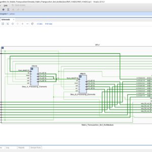
Parallel Pipelined Architecture and Algorithm for Matrix Transposition Using Registers
Base Paper Abstract:
In this brief, we present a new algorithm and architecture for continuous-flow matrix transposition using registers. The algorithm supports P-parallel matrix transposition. The hardware architecture reaches the theoretical minimums in terms of latency and memory. It is composed of a group of identical cascaded basic swap circuits, whose stages are determined by the corresponding algorithm, and can be controlled via a set of counters. Compared with the state-of-the-art architecture, the proposed architecture supports matrices whose rows and columns are integer multiples of P. Here P can be arbitrary, including but not limited to power-of-two integers. Moreover, our results provide additional insight into continuous-flow non-square matrix transposition.
List of the following materials will be included with the Downloaded Backup: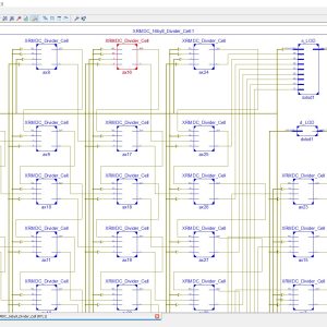
Power Efficient Approximate Divider Architecture for Error Resilient Applications
Base Paper Abstract:
Approximate computing is an emerging paradigm in error-tolerant applications that leads to power-efficient designs without significant loss in quality. The divider in these applications have complex hardware and more latency among the computational blocks resulting in power consumption. Hence approximating the division module would lead to designs with vastly improved power efficiency. A new approximate subtractor (AxSUB) is proposed in this paper with the intent to reduce the hardware complexity while achieving accuracy within permissible limits. The proposed AxSUB and existing approximate subtractor units are used in the restoring array division (RAD) architecture to prove the efficacy of the AxSUB. Comprehensive error and synthesis analysis are performed on RAD architectures implemented using AxSUB, and existing methods. Our proposed design achieved a 21% decrease in area and a 28% decrease in power consumption compared to the exact design. The proposed and existing RAD architectures is implemented on change detection applications to validate the quality-effort tradeoff.
List of the following materials will be included with the Downloaded Backup:
Power Efficient Tiny Yolo CNN Using Reduced Hardware Resources Based on Booth Multiplier and WALLACE Tree Adders
Base Paper Abstract:
Convolutional Neural Network (CNN) has attained high accuracy and it has been widely employed in image recognition tasks. In recent times, deep learning-based modern applications are evolving and it poses a challenge in research and development of hardware implementation. Therefore, hardware optimization for efficient accelerator design of CNN remains a challenging task. A key component of the accelerator design is a processing element (PE) that implements the convolution operation. To reduce the amount of hardware resources and power consumption, this article provides a new processing element design as an alternate solution for hardware implementation. Modified BOOTH encoding (MBE) multiplier and WALLACE tree-based adders are proposed to replace bulky MAC units and typical adder tree respectively. The proposed CNN accelerator design is tested on Zynq-706 FPGA board which achieves a throughput of 87.03 GOP/s for Tiny-YOLO-v2 architecture. The proposed design allows to reduce hardware costs by 24.5% achieving a power efficiency of 61.64 GOP/s/W that outperforms the previous designs.
List of the following materials will be included with the Downloaded Backup: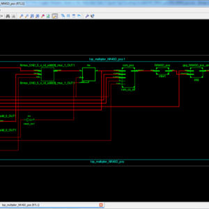
Pre Encoded Multipliers Based on Non Redundant Radix 4 Signed Digit Encoding
Abstract: In this paper we are discussed about the new design of pre-encoded multiplier are explored at offline the standard co efficient and storing them in system memory. The co efficient is used in non redundant radix 4 signed digit form. This encoding technique is less complex partial product implementation and more area and power efficient design. Analysis is verifies the proposed system is efficient from the existing system.
List of the following materials will be included with the Downloaded Backup:Provide Wordlwide Online Support
We can provide Online Support Wordlwide, with proper execution, explanation and additionally provide explanation video file for execution and explanations.
24/7 Support Center
NXFEE, will Provide on 24x7 Online Support, You can call or text at +91 9789443203, or email us nxfee.innovation@gmail.com
Terms & Conditions:
Customer are advice to watch the project video file output, and before the payment to test the requirement, correction will be applicable.
After payment, if any correction in the Project is accepted, but requirement changes is applicable with updated charges based upon the requirement.
After payment the student having doubts, correction, software error, hardware errors, coding doubts are accepted.
Online support will not be given more than 3 times.
On first time explanation we can provide completely with video file support, other 2 we can provide doubt clarifications only.
If any Issue on Software license / System Error we can support and rectify that within end of day.
Extra Charges For duplicate bill copy. Bill must be paid in full, No part payment will be accepted.
After payment, to must send the payment receipt to our email id.
Powered by NXFEE INNOVATION, Pondicherry.
Call us today at : +91 9789443203 or Email us at nxfee.innovation@gmail.com
NXFEE Development & Services

Product Categories
- 2014 (11)
- 2015 (39)
- 2016 (30)
- 2017 (16)
- 2018 (17)
- 2019 (42)
- 2020 (29)
- 2021 (17)
- 2022 (23)
- Accessories (43)
- Area Efficient (116)
- High speed VLSI Design (56)
- IEEE (15)
- Image Processing (40)
- Low power VLSI Design (97)
- NOC VLSI Design (2)
- VLSI (249)
- VLSI 2023 (21)
- VLSI 2024 (18)
- VLSI 2025 (30)
- VLSI 2026 (3)
- VLSI Application / Interface and Mini Projects (31)
- VLSI_2023 (15)
Filter by price
Product Status
Sort by rating
Sort by producents

Copyright © 2026 Nxfee Innovation.